Pyramid-shaped capacitor structure and its manufacturing method

A capacitor structure, metal technology, applied in capacitors, semiconductor/solid-state device manufacturing, circuits, etc., can solve the problems of general products being inappropriate and inconvenient

Active Publication Date: 2006-10-04
TAIWAN SEMICON MFG CO LTD
View PDF0 Cites 4 Cited by
  • Summary
  • Abstract
  • Description
  • Claims
  • Application Information

AI Technical Summary

Problems solved by technology

[0010] It can be seen that the above-mentioned existing capacitor structure obviously still has inconvenience and defects in product structure, manufacturing method and use, and needs to be further improved urgently.
In order to solve the problems existing in the capacitor structure, relevant manufacturers have tried their best to find a solution, but no suitable design has been developed for a long time, and there is no suitable structure for general products to solve the above problems. This is obviously a problem. Issues that relevant industry players are eager to solve

Method used


Image

  • Pyramid-shaped capacitor structure and its manufacturing method
  • Pyramid-shaped capacitor structure and its manufacturing method
  • Pyramid-shaped capacitor structure and its manufacturing method

Examples


Embodiment Construction

[0080] For further elaborating the technical means and effect that the present invention takes for reaching the intended invention purpose, below in conjunction with accompanying drawing and preferred embodiment, to its specific implementation, structure, manufacturing method, Steps, features and effects thereof are described in detail below.

[0081] Through the description of the specific implementation mode, when the technical means and effects adopted by the present invention to achieve the predetermined purpose can be obtained a deeper and more specific understanding, but the attached drawings are only for reference and description, and are not used to explain the present invention be restricted.

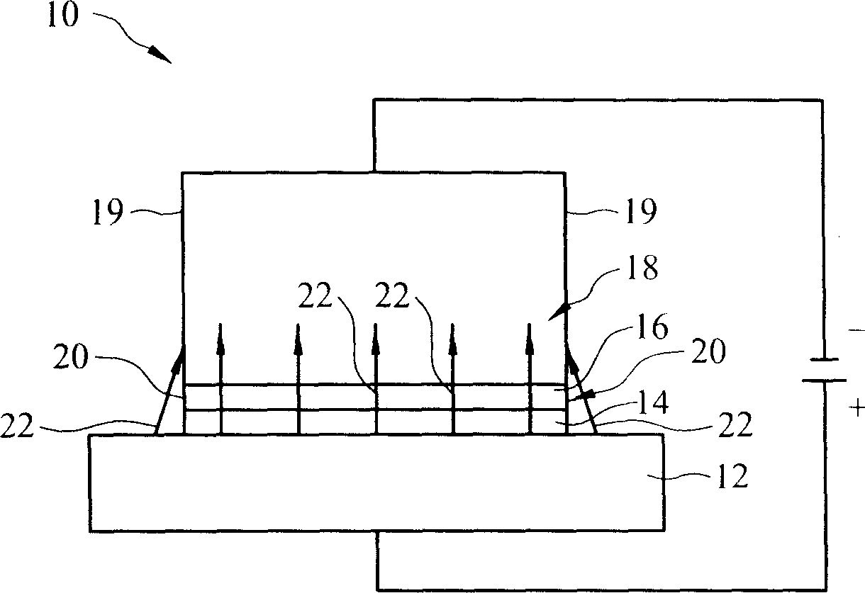
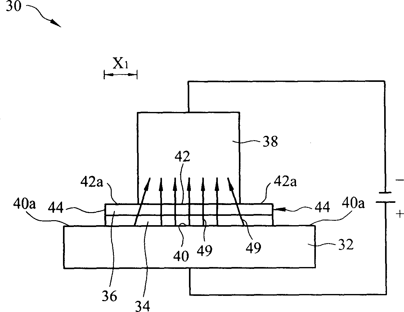
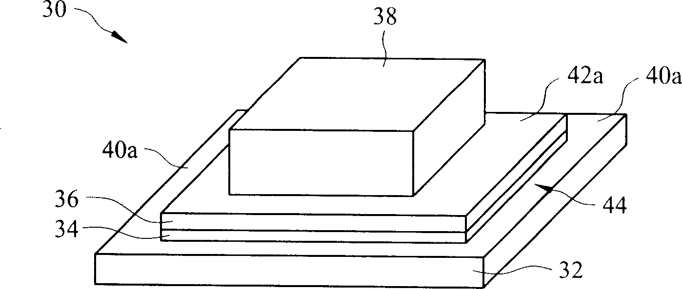
[0082] The present invention proposes a capacitive structure with a generally pyramidal profile. The capacitor structure includes a lower conductive layer, an upper conductive layer, and at least one dielectric layer between the lower conductive layer and the upper conductive ...


PUM


Abstract

A capacitor structure which has a generally pyramidal or stepped profile to prevent or reduce dielectric layer breakdown is disclosed. The capacitor structure includes a first conductive layer, at least one dielectric layer having a first area provided on the first conductive layer and a second conductive layer provided on the at least one dielectric layer. The second conductive layer has a second area which is less than the first area of the at least one dielectric layer. A method of fabricating a capacitor structure is also disclosed.

Description

technical field [0001] The present invention relates to a semiconductor element and a method for manufacturing the element, in particular to a pyramid-shaped capacitor structure in a semiconductor element, and a pyramid-shaped capacitor structure that is more resistant to edge breakdown (EdgeBreakdown) and its manufacture method. Background technique [0002] In the manufacture of semiconductor integrated circuits, metal conductor lines are used to interconnect (Interconnect) multiple components in the component circuits on the semiconductor wafer. The general process used to deposit metal conductor patterns on semiconductor wafers includes: depositing a conductive layer on a silicon wafer substrate; using standard lithography techniques to form a photoresist or other masks, such as titanium oxide or silicon oxide; subjecting the wafer substrate to a dry etching process to remove the conductive layer from areas not covered by the mask, leaving a masked metal layer in the fo...

Claims


Application Information

Patent Timeline
Patent Type & Authority Applications(China)
IPC IPC(8): H01L27/00H01L27/02H01L27/06H01L27/102H01L27/108H01L29/92H01L21/00H01L21/02H01L21/82H01L21/8222H01L21/8242
CPCH01L28/60
Inventor 黄坤铭汪业杰陈盈德朱翁驹陈富信吴子扬
Owner TAIWAN SEMICON MFG CO LTD
Why Eureka
Try Eureka