

Mass TDMA complex switching chip data processing method
A technology of time division multiplexing and switching chips, applied in time division multiplexing systems, multiplexing communications, electrical components, etc., can solve the problems of high cost, complex implementation and control, poor reliability, etc. Low, simple to implement and control, high reliability
- Summary
- Abstract
- Description
- Claims
- Application Information
AI Technical Summary
Problems solved by technology
Method used
Image

Examples
Embodiment Construction
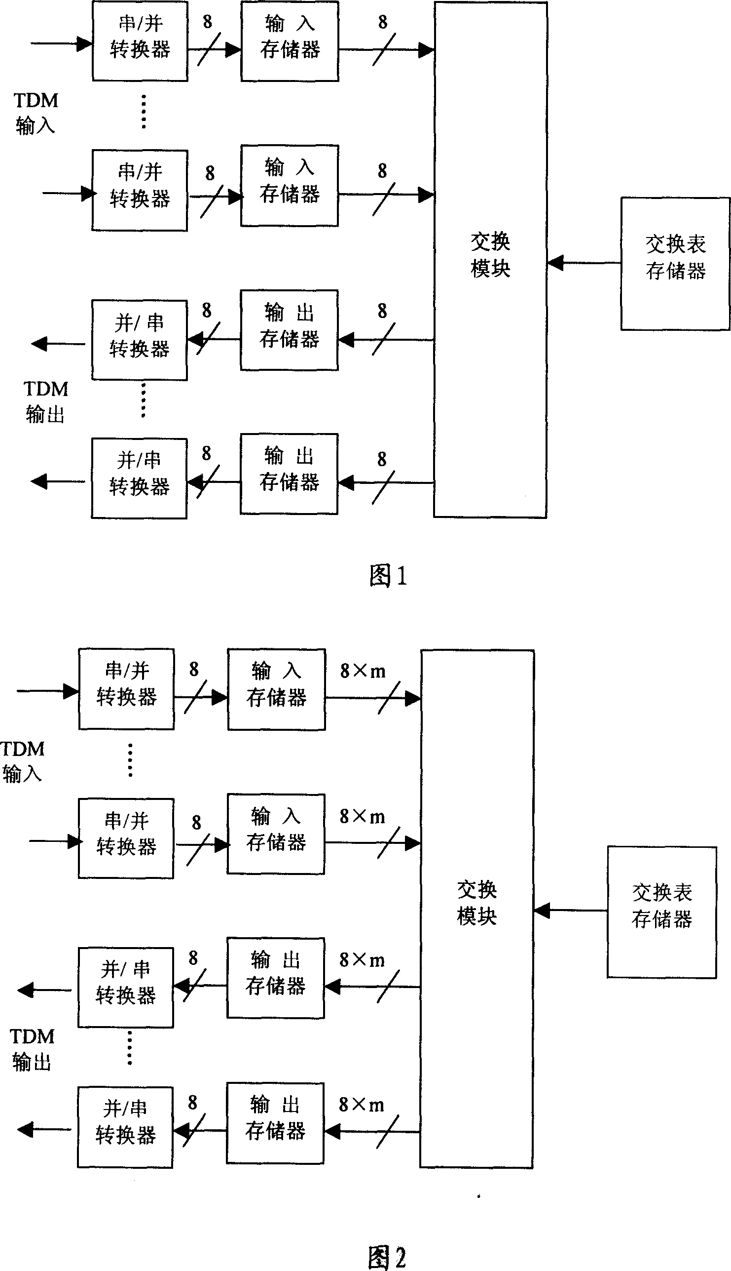
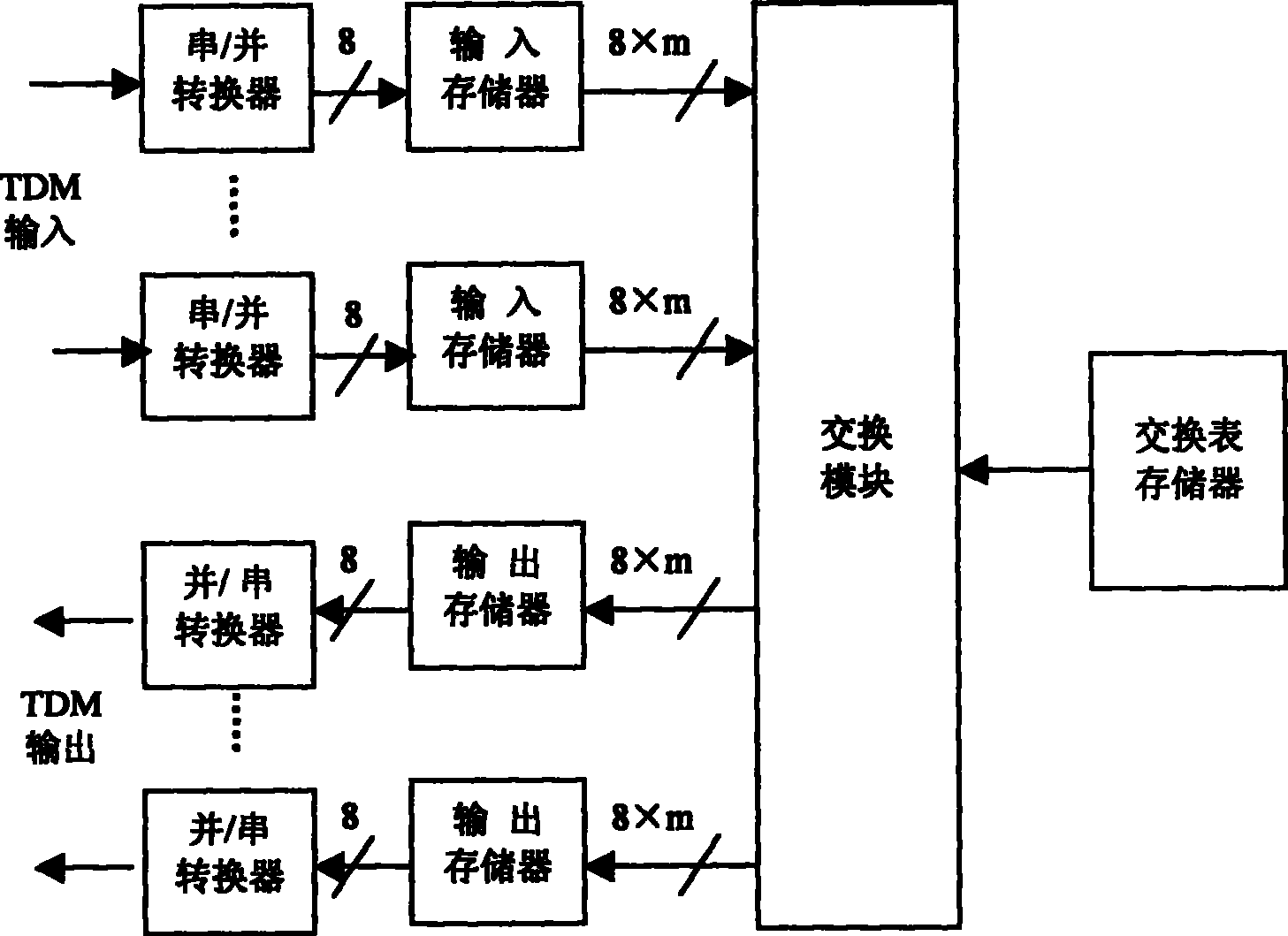
[0020] The core of the present invention is that the write data bit width of the input memory is 8, and the read data bit width is 8 × m; the write data bit width of the output memory is 8 × m, and the read data bit width is 8; the input memory and The output memory simultaneously completes the functions of data buffering and bit width conversion, and the switching module processes a bit width of 8×m, so that the capacity of the TDM switching chip is m times that of the prior art solution.
[0021] The specific embodiment of the device of the present invention is as shown in Figure 2, the structure of described high-capacity TDM switch chip device comprises: serial / parallel converter, parallel / serial converter, input memory, output memory, exchange module and swap table memory;
[0022] The connection relationship between the modules included in the device will be further described below in conjunction with the data input and output processing process:
[0023] The device rec...
PUM
 Abstract
Description
Claims
Application Information