
Driver for display apparatus and display apparatus including the same

A display device and driver technology, applied in static indicators, instruments, static memory, etc., can solve problems such as flicker, voltage difference, and spotting on the screen

Inactive Publication Date: 2007-03-14
SAMSUNG ELECTRONICS CO LTD
View PDF0 Cites 14 Cited by
  • Summary
  • Abstract
  • Description
  • Claims
  • Application Information

AI Technical Summary

Problems solved by technology

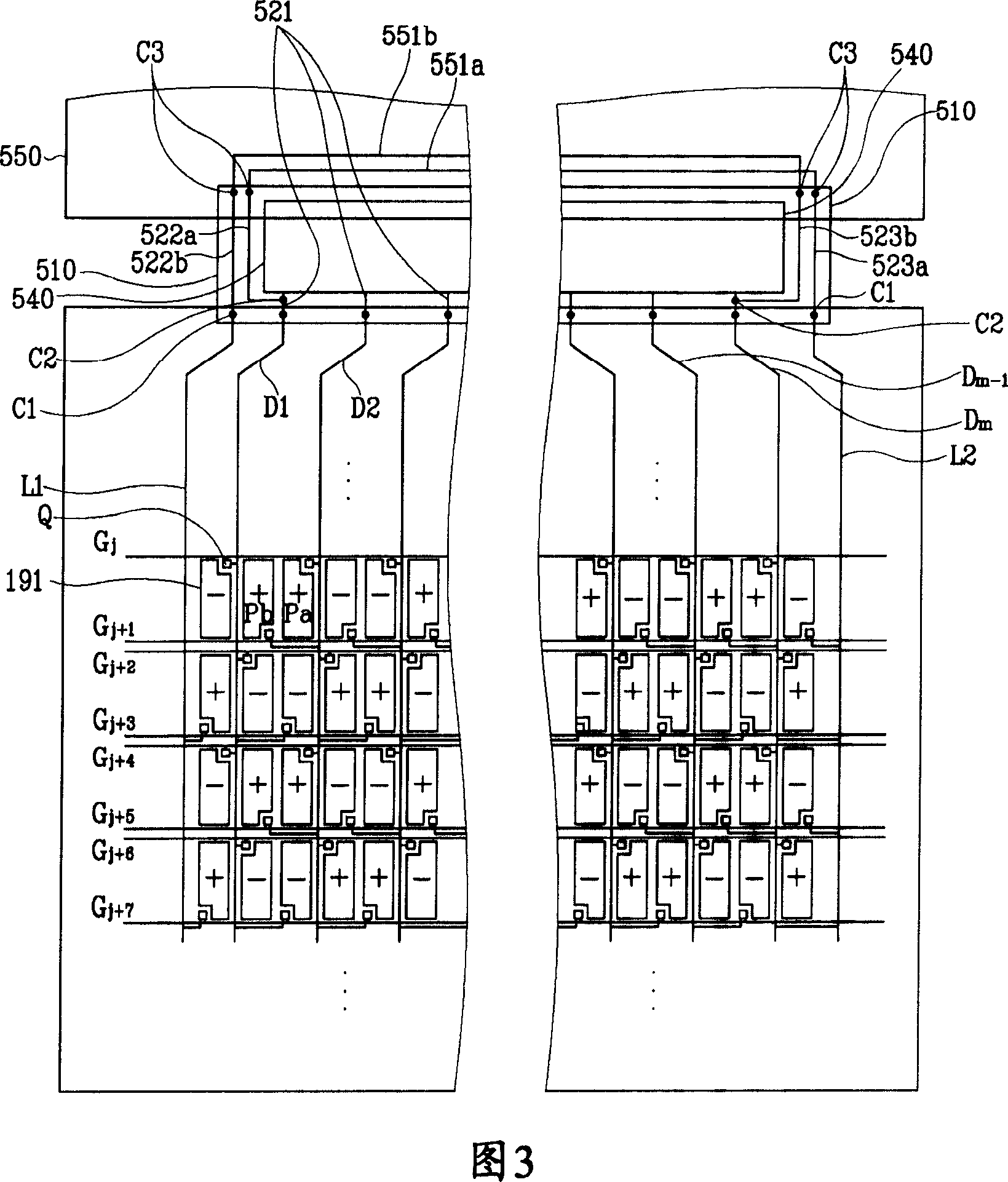
This creates a voltage difference between positive and negative pixel voltages, causing flicker
Also, the screen may be stained due to residual images or fingerprints

Method used


Image

  • Driver for display apparatus and display apparatus including the same
  • Driver for display apparatus and display apparatus including the same
  • Driver for display apparatus and display apparatus including the same

Examples


Embodiment Construction

[0037] The present invention will be described more fully below with reference to the accompanying drawings. However, the present invention can be implemented in many different ways and is not limited to the embodiments described here. Rather, these embodiments are provided so that those skilled in the art will fully disclose and fully cover the scope of the present invention. Like reference numbers indicate similar elements.

[0038] It will be understood that when an element is referred to as being "on" another element, it can be directly on the other element or intervening elements may also be present. In contrast, when an element is referred to as being "directly on" another element, there are no intervening elements present. As used herein, the term "and / or" includes any and all combinations of one or more of the associated listed items.

[0039] It should be understood that, although the terms first, second, third, etc. may be used herein to describe various elements,...


PUM

PropertyMeasurementUnit
hysteresis lossaaaaaaaaaa

Abstract

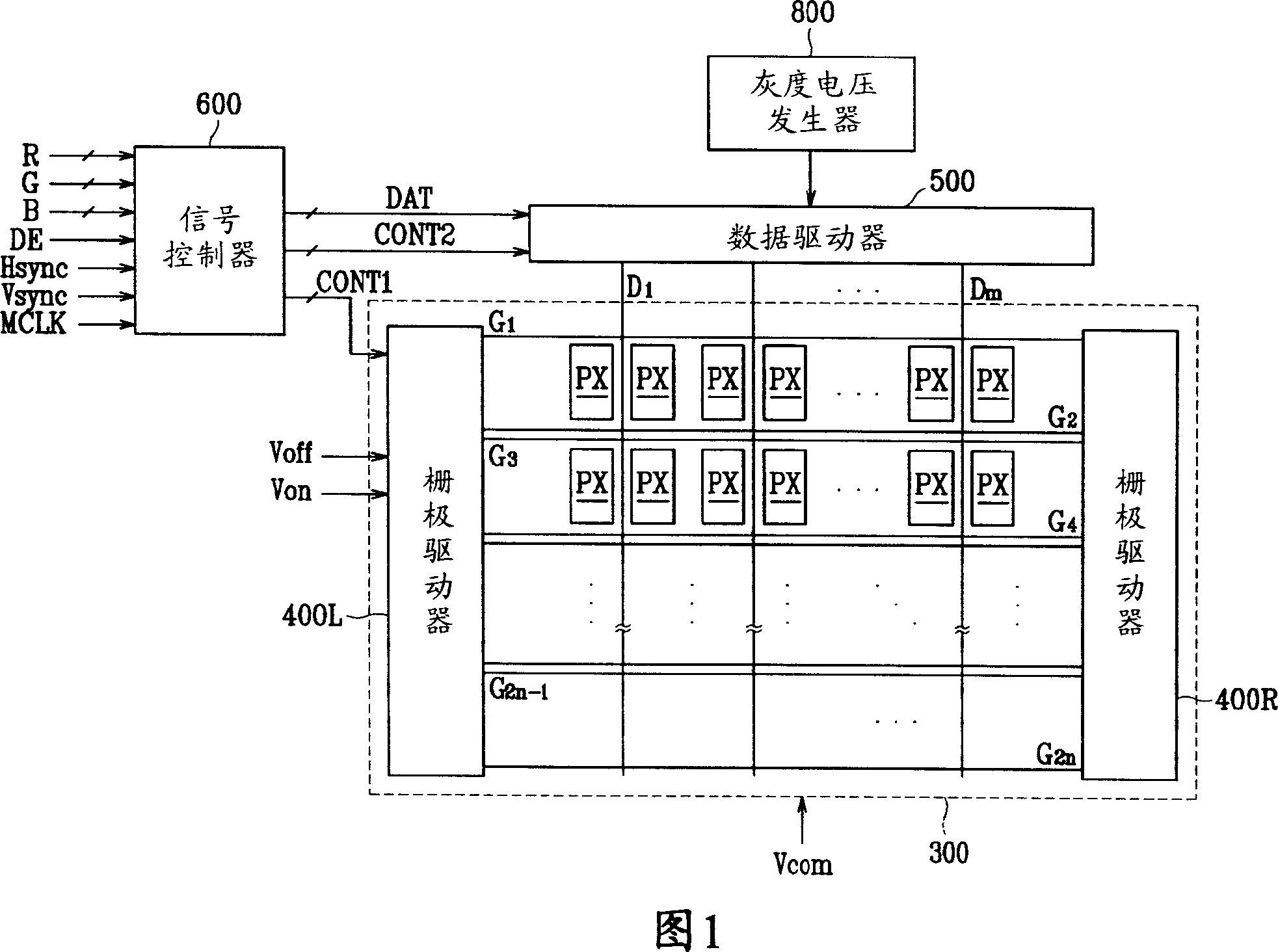
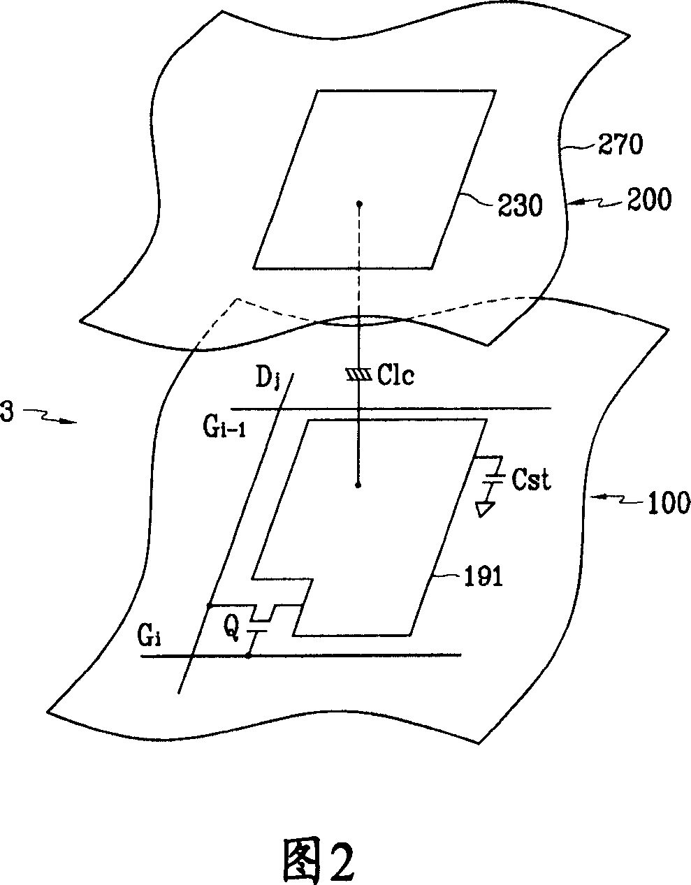
Provided is a driver for a display apparatus and a display apparatus having the same. The driver includes a plurality of gate lines that transmit gate signals, and first and second gate drivers that are respectively connected to odd-numbered and even-numbered gate lines among the plurality of gate lines and generate the gate signals based on a plurality of clock signals, wherein two adjacent clock signals among the plurality of clock signals have a phase difference equal to or greater than 180 DEG and less than 360 DEG . Accordingly, voltage drop caused by a kickback voltage occurs only one time by allowing two adjacent clock signals to have a predetermined time delay from each other, so that a positive data voltage is the same as a negative data voltage, thereby preventing flicker or stain.

Description

[0001] This application claims priority from Korean Patent Application No. 2005-0083039 filed with the Korean Intellectual Property Office on Sep. 7, 2005, the entire contents of which are hereby incorporated by reference. technical field [0002] The present invention relates to a driver for a display device and a display device having the driver. Background technique [0003] In general, a liquid crystal display (LCD) device includes two panels provided with pixel electrodes and common electrodes, and a liquid crystal layer having dielectric anisotropy disposed between the two panels. The pixel electrodes are arranged in a matrix. The pixel electrodes are connected to switching elements such as thin film transistors ("TFTs") to be sequentially applied with data voltages in units of pixel rows. The common electrode is provided over the entire surface of the panel, and is applied with a common voltage. According to the circuit principle, the pixel electrode, the common ele...

Claims


Application Information

Patent Timeline
Patent Type & Authority Applications(China)
IPC IPC(8): G09G3/36G09G3/20G02F1/133
CPCG11C19/28G09G2310/0251G09G2320/0209G09G3/3614G09G2310/08G09G3/3677G09G3/3648G09G2300/0426G09G3/36G09G3/20G02F1/13
Inventor 金圣万
Owner SAMSUNG ELECTRONICS CO LTD
Learn More