Chopper amplifier circuit and semiconductor device

一种斩波放大器、电路的技术,应用在放大器、低频放大器、改进放大器以减少温度/电源电压变化等方向,能够解决压电晶体管不完全匹配、无法消除传感器桥偏移电压等问题

Inactive Publication Date: 2007-03-14
SII SEMICONDUCTOR CORP +1
View PDF1 Cites 14 Cited by
  • Summary
  • Abstract
  • Description
  • Claims
  • Application Information

AI Technical Summary

Problems solved by technology

When using a conventional chopper amplifier circuit, for example for amplifying the output voltage of a sensor bridge using piezo transistors, the offset voltage of the sensor bridge cannot be canceled due to the imperfect matching of the piezo transistors

Method used


Image

  • Chopper amplifier circuit and semiconductor device
  • Chopper amplifier circuit and semiconductor device
  • Chopper amplifier circuit and semiconductor device

Examples


no. 1 example

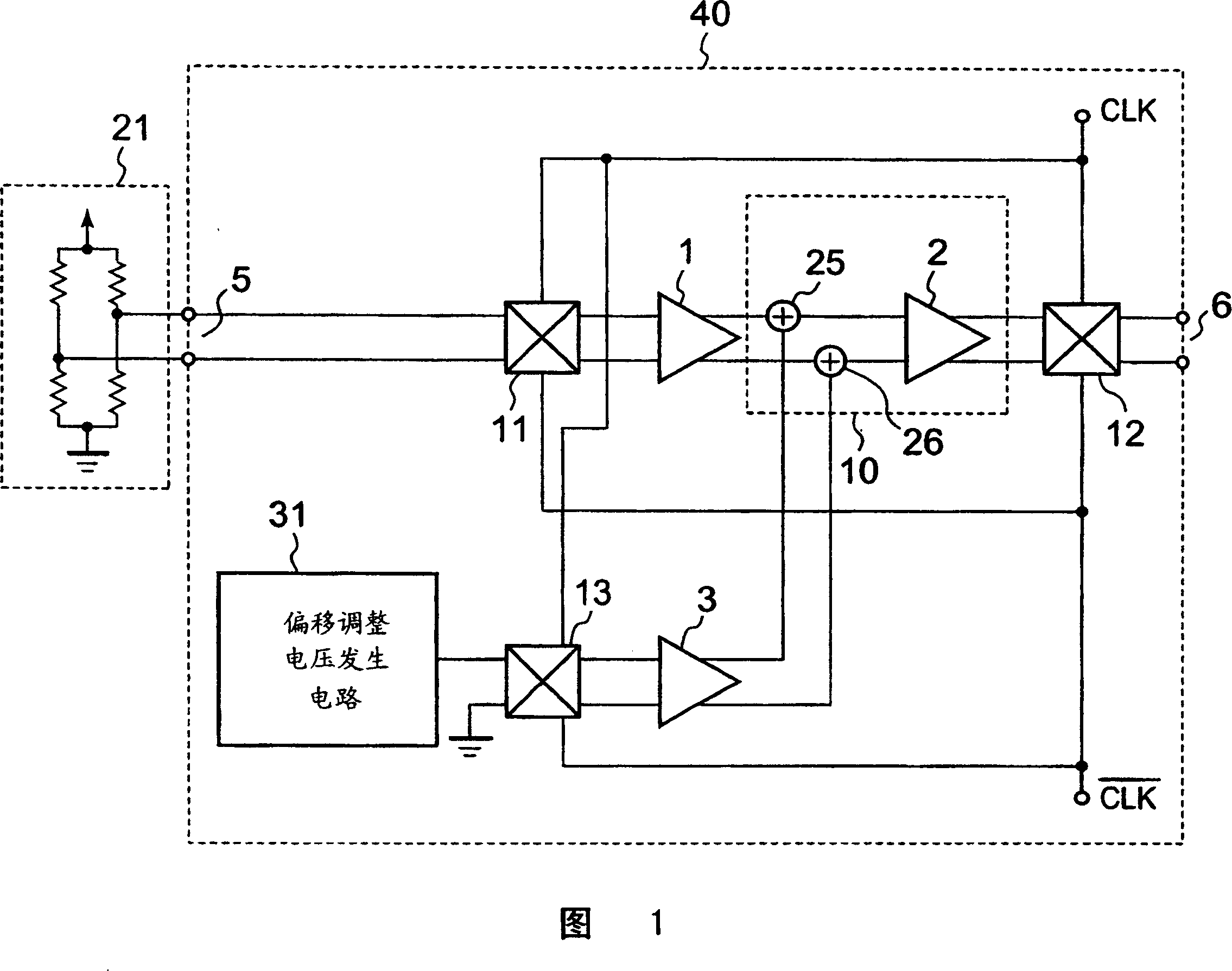
[0020] FIG. 1 is a block diagram of a chopper amplifier circuit according to a first embodiment of the present invention.

[0021] The chopper amplifier 40 receives the sensor signal from the sensor bridge 21 at the input terminal 5 and outputs an amplified signal from the output terminal 6 . The sensor signal input to the input 5 is chop-modulated by the modulation signal CLK in the multiplier 11 and then amplified in the amplifier circuit 1 . The offset adjustment voltage generating circuit 31 generates an offset adjustment voltage, the amplitude of which is the same as that of the offset voltage of the sensor bridge 21 but opposite in polarity. The offset adjustment voltage is chopped and modulated by the modulation signal CLK in the multiplier 13 and amplified in the amplification circuit 3 . The adders 25 and 26 add the above-mentioned sensor signal to the offset adjustment voltage, thereby canceling the offset voltage of the sensor bridge 21 in the sensor signal. In ad...

no. 2 example

[0030] FIG. 5 is a block diagram of a chopper amplifier circuit according to a second embodiment of the present invention.

[0031] Typically, the offset voltage of a sensor bridge has a temperature characteristic. As an example here, it is assumed that the offset voltage of the sensor bridge has a temperature characteristic as shown in FIG. 7 .

[0032] In the second embodiment, an offset temperature characteristic adjustment voltage generation circuit 32 is provided in addition to the chopper amplifier circuit of the first embodiment. The offset temperature characteristic adjustment voltage generating circuit 32 outputs an offset temperature characteristic adjustment voltage whose characteristic is equal to the temperature characteristic of the offset voltage of the sensor bridge. The offset temperature characteristic adjustment voltage is chop-modulated by the multiplier 14 and amplified by the amplifying circuit 4, and then added to the chop-modulated sensor output signal...


PUM


Abstract

The present invention provides a chopper amplifier circuit capable of reducing the offset voltage of a sensor bridge and the temperature characteristic of the offset voltage. An offset adjustment voltage generating circuit is provided for generating a voltage equal to the offset voltage of the sensor bridge, and an offset temperature characteristic adjusting voltage generating circuit is provided for generating a voltage having the same temperature characteristic as the offset voltage. These output voltages are chop modulated and subtracted from the chop modulated output signal of the sensor bridge.

Description

technical field [0001] The present invention relates to a chopper amplifier circuit and a semiconductor device including the chopper amplifier circuit. Background technique [0002] FIG. 2 is a block diagram showing a conventional chopper amplifier circuit. In the conventional chopper amplifier circuit 20, multipliers 11 and 12 are provided at the front end and rear end of the amplifier circuit 1, respectively. The multipliers 11 and 12 are controlled by a square wave modulation signal CLK having a frequency fc. The output of this chopper amplifier circuit 20 is connected to a low pass filter 22 (see P. Allen and D.R. Holberg, CMOS Analog Circuit Design, P490-494, Saunders College Publishing, 1987). [0003] 3A to 3F show frequency characteristics of input signals in various parts of a conventional chopper amplifier circuit. Assume that the input signal has a frequency characteristic at the input terminal 5 of the chopper amplifier circuit 20 as shown in FIG. 3A. In addi...

Claims


Application Information

Patent Timeline
Patent Type & Authority Applications(China)
IPC IPC(8): H03F1/30H03F3/187
CPCH03F3/45775
Inventor 吉泽浩和安斋亮一内田俊之有山稔五十岚敦史武田晃
Owner SII SEMICONDUCTOR CORP
Why Eureka
Try Eureka