Driver of plasma display screen

A technology of plasma display screen and driving device, which is applied in the direction of identification device, static indicator, instrument, etc. It can solve problems such as hindering stable operation, poor screen brightness, and the probability of component damage, so as to reduce the impact and eliminate brightness difference. Effect

Inactive Publication Date: 2007-04-04
LG电子(南京)等离子有限公司
View PDF0 Cites 2 Cited by
  • Summary
  • Abstract
  • Description
  • Claims
  • Application Information

AI Technical Summary

Problems solved by technology

[0011] At this time, there are more unselected channels than selected channels, so the wasted power consumption due to grounding becomes larger
Since the first switching elements (211-2 to 211-n) and the grounding switching element 230 are turned on, the voltage drop caused by the line impedance of the Y electrode causes a brightness difference between the left and right sides of the screen.
In addition, the probability of component damage due to power fluctuations inside the IC block increases
[0012] Moreover, in the scanning process or support process, according to the voltage standard level of each electrode, the change of the dynamic load (dynamic load) generated during discharge will affect the adjacent electrodes, causing noise (noise), or the pulse generated during discharge The effect of the flow into adjacent electrodes or cells causes unstable operation
[0013] For example, since the first switching elements (211-2 to 211-n) of the scan driver associated with the unselected channels are turned on and grounded, a large current will flow during the scanning process, and this large current will affect Adjacent cells or adjacent electrodes can cause noise or prevent stable operation

Method used


Image

  • Driver of plasma display screen
  • Driver of plasma display screen
  • Driver of plasma display screen

Examples


Embodiment Construction

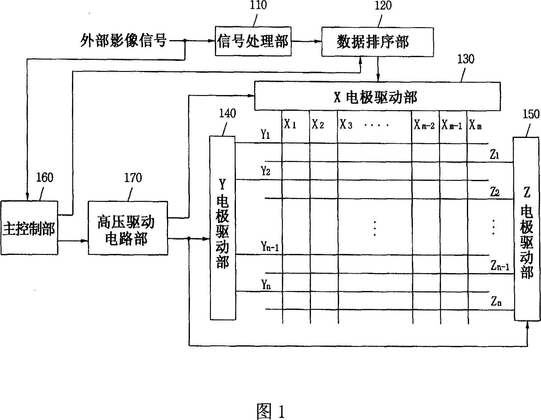
[0022] 下面将参照附图对本发明的实施例进行详细说明。

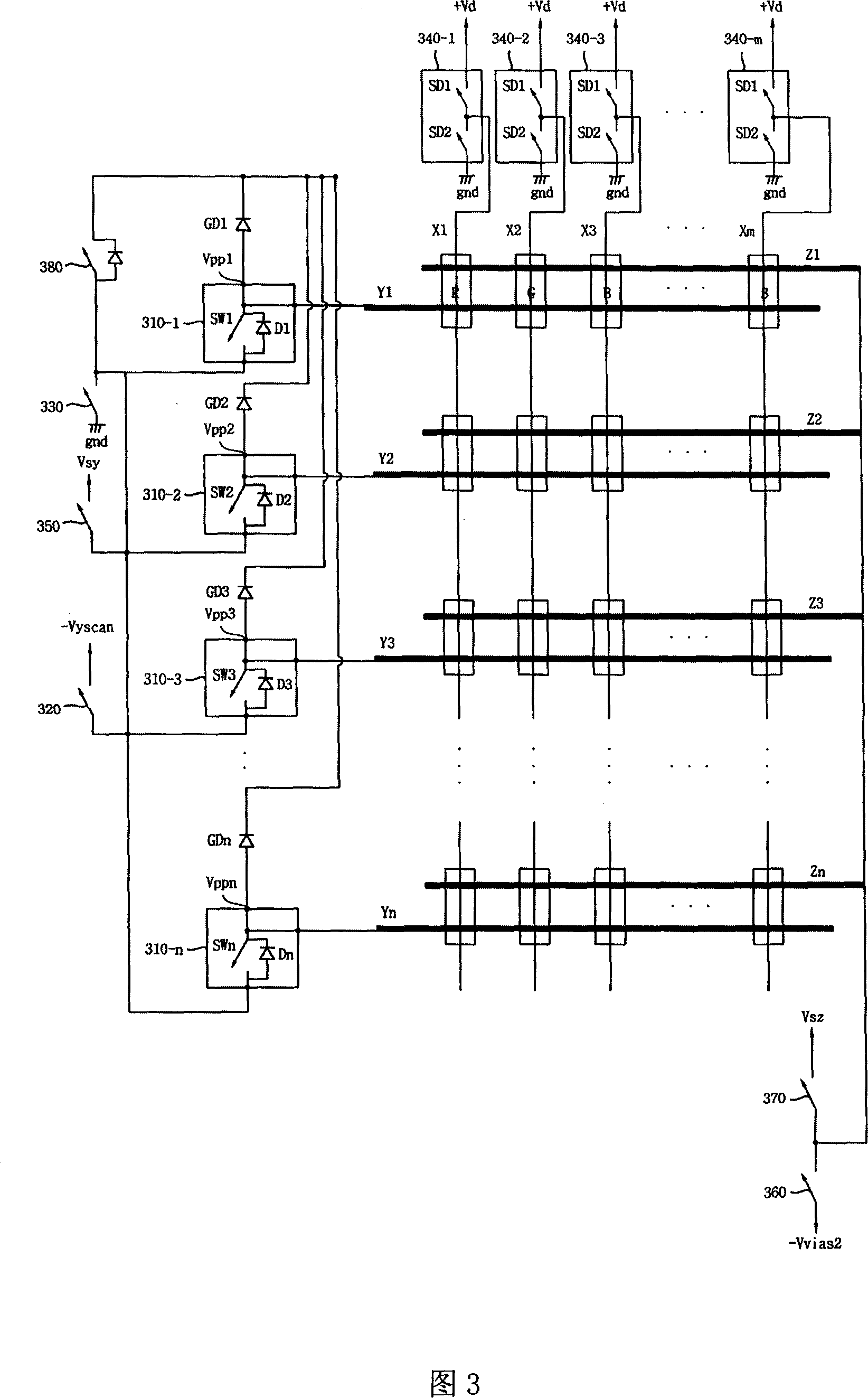
[0023] 图3是本发明的等离子显示屏的驱动装置电路图。下面参照图3对扫描过程和支持过程中本发明的驱动装置的操作进行说明。

[0024] 首先,在扫描过程中,与被选择的Y电极(Y1至Yn之一)相关的扫描驱动器(310-1至310-n之一)的开关元件(SW1至SWn之一)被开启,而未被选择的其余扫描驱动器的开关元件和接地用开关元件330、380被关闭,另外数据驱动器(340-1至340-m)的数据开关元件SD1和扫描用开关元件320被开启。

[0025] 这样,向X电极(X1至Xm)施加数据驱动器(340-1至340-m)的输出(+Vd),而向被选择的Y电极(Y1至Yn之一)则施加-Vyscan,以对位于被选择的Y电极(Y1至Yn之一)上的单元(cell)进行数据的写入。

[0026] 此时,由于接地用开关元件330、380和未被选择的其余扫描驱动器的开关元件被关闭,所以除被选择的Y电极(Y1至Yn之一)外的其余Y电极处于浮接状态。

[0027] 例如,与第1个Y电极Y1相关的扫描驱动器310-1的开关元件SW1被开启,而未被选择的其余扫描驱动器(310-2至310-n)和接地用开关元件被关闭。另外,数据驱动器(340-1至340-m)的数据用开关元件SD1和扫描用开关元件320被开启。这样,在第1个Y电极Y1将施加-Vyscan,在X电极(X1至Xm)施加+Vd,从而在存在于第1个Y电极Y1上的单元内发生Vyscan+Vd的电压差,以进行数据写入。此时,由于接地用开关元件330、380和未被选择的其余扫描驱动器(310-2至310-n)的开关元件(SW2至SWn)被关闭,所以除第1个Y电极Y1外的其余Y电极(Y2至Yn)处于浮动状态。

[0028] 如上所述,由于未被选择的Y电极处于浮接状态,所以不会产生现有技术中由电极线阻抗带来的电压下降,从而可消除画面左右的亮度差,改善画质。

[0029] 不仅如此,由于未被选择的Y电极处于浮接状态,所以在扫描过程中,不会产生未被选择的扫描驱动器上的被开启的第1开关元件接地而造成大电流,因此能够解决由噪音所带来的许多问题。

[0030] 于是,在对所有Y电极(Y1至Yn)完成扫描过程后进行支持过程。

[0...


PUM


Abstract

A driving device for plasma display includes X electrodes enforcing data pulse, Y electrodes enforcing scanning and maintaining pulse, Z electrodes enforcing coordinate supporting pulse. There is a switch on each Y electrode, at one of the switch open scanning pulse is enforced to the selected electrode, the other switches are closed. This invention decreases noise and the discharge effect and eliminate brightness difference caused by coil impedance.

Description

technical field [0001] 本发明是关于等离子显示屏的,更具体地说是关于等离子显示屏的驱动装置。 Background technique [0002] 图1是普通等离子显示屏的驱动装置构成框图。如图1所示,信号处理部110把从外部输入的影像信号转换成适合等离子显示屏驱动的影像数据。 [0003] 数据排序部120为了对通过信号处理部110转换的影像数据进行灰度级(gray scale)处理,将一个域TV影像数据重新构成为复数子域(subfield)。 [0004] X电极驱动部130和Y电极驱动部140将用于在等离子显示屏的放电单元上形成壁电压的地址脉冲和扫描脉冲,分别施加到X电极和Y电极上。Y电极驱动部140和Z电极驱动部150则分别向Y电极和Z电极交替施加支持脉冲,支持脉冲用于维持形成由有壁电压的放电单元(cell)的放电。 [0005] 主控制部160根据外部影像信号,来控制在数据排序部重新排序的影像数据按顺序判读,向X电极驱动部130提供1扫描线分量,同时将逻辑控制脉冲施加到高压驱动电路部170。 [0006] 高压驱动电路部170负责从主控制部160接收逻辑控制脉冲,并将高压控制脉冲加到X电极、Y电极及Z电极驱动部130、140、150。 [0007] 此时,Y电极驱动部140为了向Y电极上施加扫描脉冲或支持脉冲,设置有如图2所示的扫描驱动器210。现有的扫描驱动器210是包含有2个开关元件的集成电路块(Integrated Circuit package)。2个开关元件形成一个信道,并向一个Y电极施加扫描脉冲或支持脉冲,所以应该使用耐压大的开关元件。现有扫描驱动器210由于由2个耐压大的开关元件组成,所以缺点是费用增加、集成电路块变大。 [0008] 另外,在扫描过程中未被扫描驱动器210选择的信道需要第1开关元件(211-1至211-n)经常开启,保持接地电平(ground level)。 [0009] 例如:在扫描过程中,如果选择与第1个Y电极Y1相关的信道,那么与其余Y电极(Y2、Y3......Yn)相关的信道则不被选择。如果这样选择信道,那么与被选择的信道相关的第1个扫描驱动器210-1的第2开关元件213-1则开启,并且扫描用的开关元件220开启。与此同时,未...

Claims


Application Information

Patent Timeline
Patent Type & Authority Applications(China)
IPC IPC(8): G09G3/28G09G3/20H01J17/49G09F9/313G09G3/291
Inventor 文成学
Owner LG电子(南京)等离子有限公司
Why Eureka
Try Eureka