
A surface discharge type aperture mask style plasma display plate with novel electrode structure
A technology of surface discharge and electrode structure, applied in cold cathode tubes, solid cathode components, etc., can solve the problems of low discharge efficiency and low brightness, and achieve the effects of improved display brightness, long discharge path, and improved luminous efficiency
- Summary
- Abstract
- Description
- Claims
- Application Information
AI Technical Summary
Problems solved by technology
Method used
Image

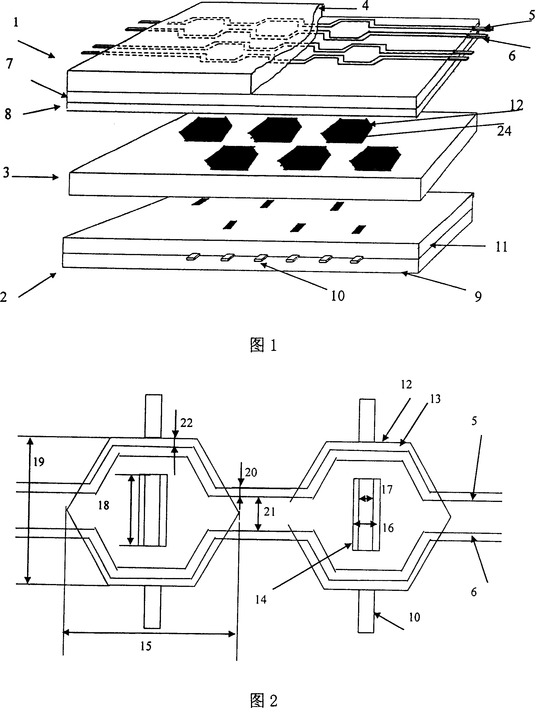
Examples
Embodiment 2
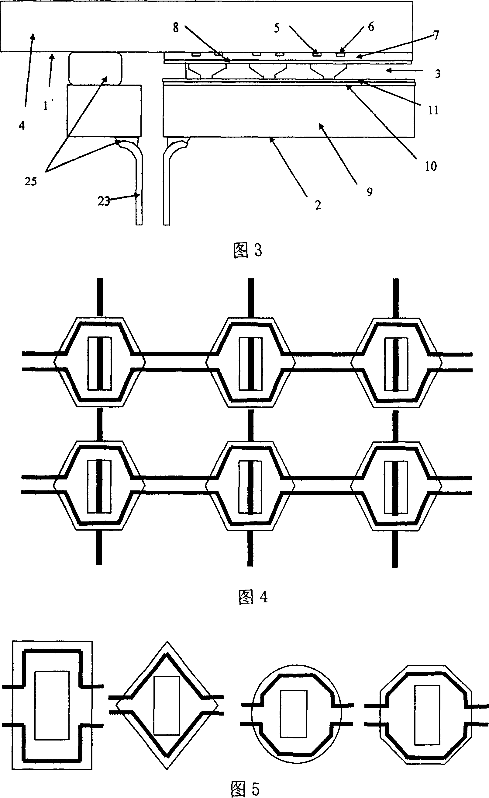
[0031] In the first embodiment above, the upper opening 13 of the grid hole 12 of the shadow mask 3 is hexagonal and arranged in a strip shape, and the first electrode pairs 5, 6 are arranged non-parallel to the discharge area of the upper opening 13, and the connection distance The first electrode pairs 5 and 6 at the shortest points are arranged in parallel, constituting the second embodiment. The grid holes 12 arranged in stripes and the relationship between the first electrode pairs 5 and 6 and the upper opening 13 are shown in FIG. 4 .
[0032] The sealing process and display principle of the display panel are the same as those in the first embodiment.
Embodiment 3
[0034] In the above-mentioned first embodiment, the shadow mask grid holes 12 form the upper openings of polygonal structures such as elongated, rhombus, circular, hexagonal or octagonal structures, and the lower openings are elongated, and the center of the upper and lower openings is within Conditions on a straight line perpendicular to the surface of the shadow mask, the corresponding first electrode pairs 5, 6 are arranged similarly to the inner edge of the upper opening 13, and the grid holes 12 of the shadow mask can be arranged in strips according to the display resolution requirements Or arranged in a Chinese character, the schematic diagram of the relationship between the front plate electrode structure and the shadow mask holes is shown in Figure 5, which constitutes the third embodiment group of the present invention, and its working principle is the same as that of the first embodiment.
Embodiment 4
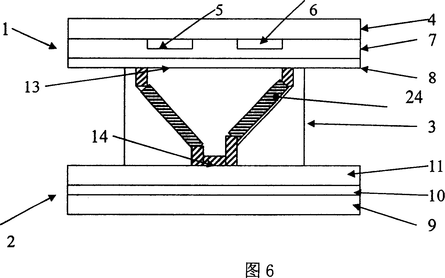
[0036] In the first, second, and third embodiments above, the monochrome phosphor powder 24 is coated on the inner wall of the shadow mask mesh hole 12 and the array formed by the surface part of the dielectric layer 11 of the rear substrate 2 corresponding to the lower opening 14, and filled with Appropriate working gas makes it generate ultraviolet light of corresponding wavelength to excite the ultraviolet phosphor to emit monochromatic visible light, thereby realizing image display, as shown in Figure 6, which constitutes the fourth embodiment group of the present invention, that is, the new electrode Structured monochrome surface-type shadow-mask plasma display panel.
PUM
 Abstract
Description
Claims
Application Information