

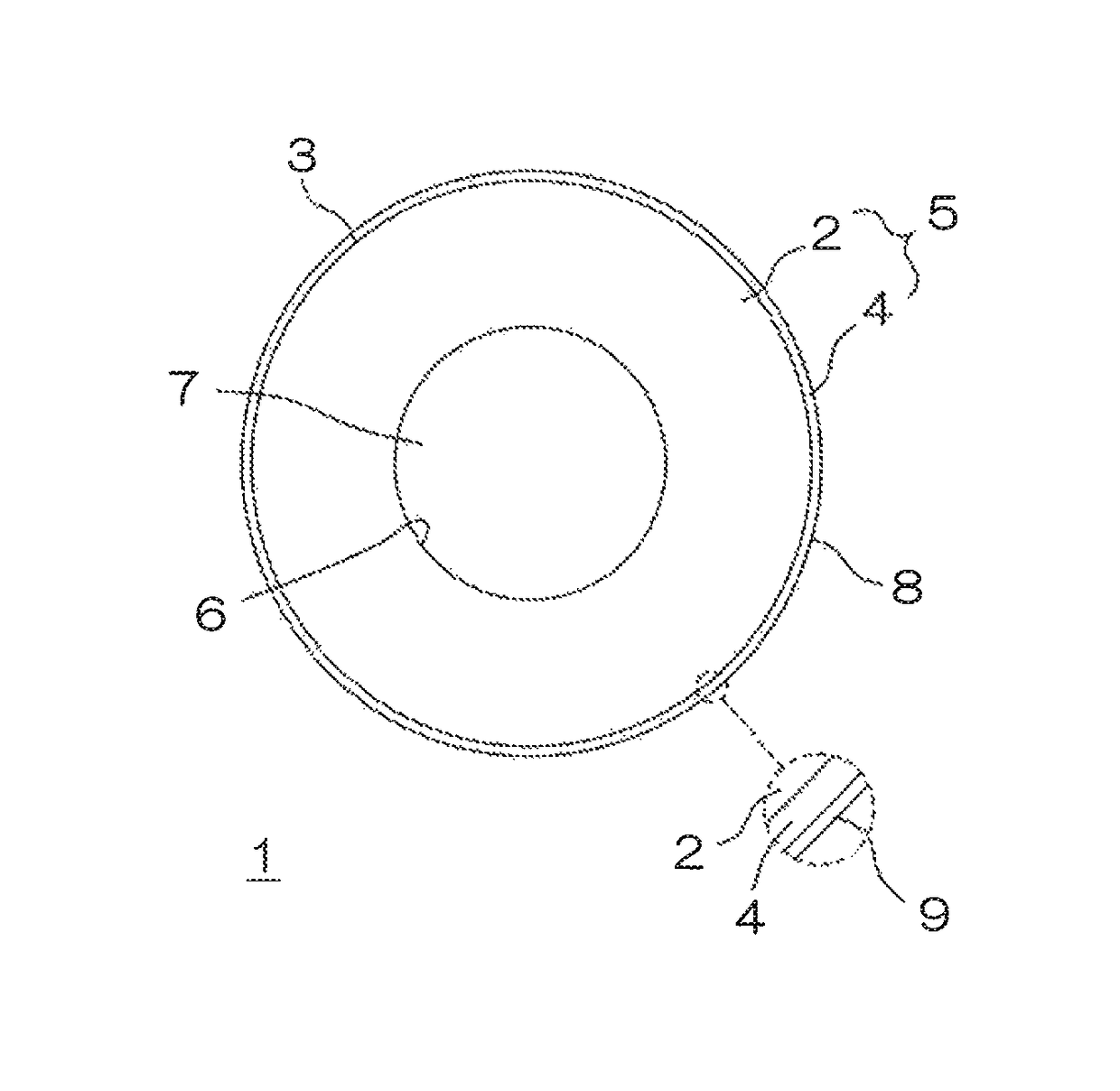
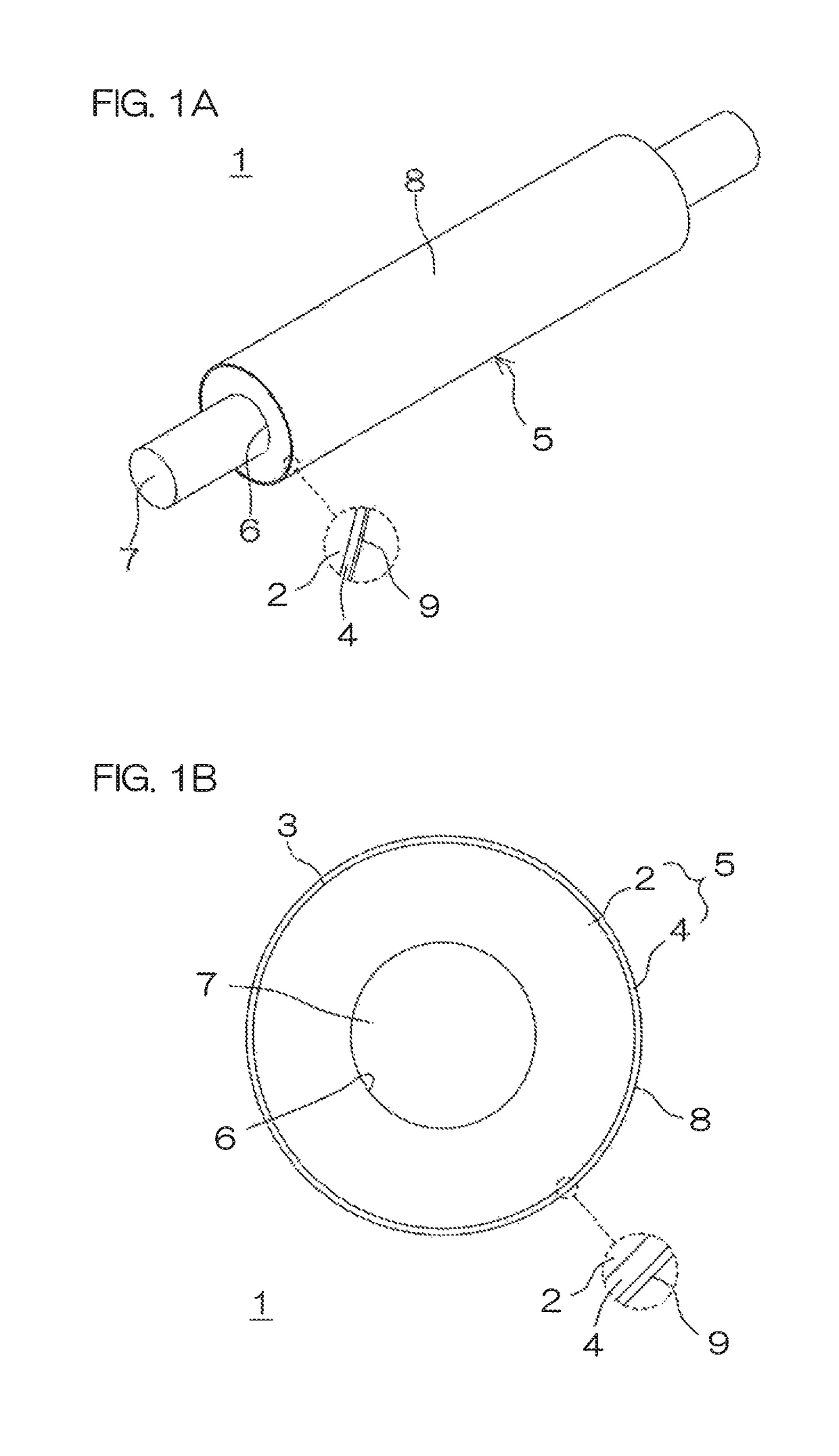
Semiconductive roller
a technology of semi-conductive rollers and conductive plates, which is applied in the direction of instruments, electrographic process equipment, optics, etc., can solve the problems of reducing the service life of toners, reducing the image density of formed images, and reducing the adhesion of toners
- Summary
- Abstract
- Description
- Claims
- Application Information
AI Technical Summary
Benefits of technology
Problems solved by technology
Method used
Image

Examples
examples
[0168]The present invention will hereinafter be described in greater detail by way of Examples and Comparative Examples but not by way of limitation.
[0169]IR (non-oil-extension type IR, Nipol (registered trade name) IR2200 available from Nippon Zeon Corporation, and having a Mooney viscosity of 82 (median)) was used as a nonpolar rubber.
[0170]While 100 parts by mass of the nonpolar rubber was simply kneaded by means of a Banbury mixer, the following ingredients were added to and further kneaded with the nonpolar rubber.
[0171]
TABLE 1IngredientsParts by massZinc oxide type-25Carbon40Petroleum-derived oil60
[0172]The ingredients shown in Table 1 are as follows. The amounts (parts by mass) of the ingredients shown in Table 1 are based on 100 parts by mass of the overall nonpolar rubber.[0173]Zinc oxide type-2: Crosslinking accelerating agent (available from Sakai Chemical Industry Co., Ltd.)[0174]Carbon: Electron conductive agent (SHOBLACK (registered trade name) N220 available from Cabo...
PUM
 Abstract
Description
Claims
Application Information