Sliding element for contacting printed circuit boards

a technology of printed circuit boards and sliding elements, which is applied in the direction of coupling contact members, coupling device connections, current collectors, etc., can solve the problems of high labor costs, large installation space requirements, and high cost of conventional cabling arrangements using plug-type connectors and cables. , to achieve the effect of not being sensitive to malfunctions and without high labor costs

Active Publication Date: 2018-12-04
HARTING ELECTRIC GMBH & CO KG
View PDF18 Cites 3 Cited by
  • Summary
  • Abstract
  • Description
  • Claims
  • Application Information

AI Technical Summary

Benefits of technology

[0006]Embodiments of the present invention provide a device for contacting two printed circuit boards. It is to be possible to move the device in a variable manner between the printed circuit boards and thus to connect and provide contact between different conducting tracks that are provided on the printed circuit boards. Moreover, it is to be possible to produce the device in a cost-effective manner and to install said device without a high expenditure of labor. In addition, it would be of advantage if the device is low-maintenance and not sensitive to malfunctions.
[0010]In one advantageous embodiment, two receiving arrangements are provided in the base body and said receiving arrangements are used to receive two contact elements. It is thus possible to configure the base body and the sliding element in a symmetrical manner.
[0011]The contact element is configured as a spring element and is preferably produced from a spring-elastic material. The contact element forms two contact limbs that can hold said contact element in the base body. Depending upon the embodiment, it is also possible to form fastening lugs directly on the contact limbs and said fastening lugs render it possible to improve the manner in which the contact element is held in the receiving arrangement of the base body.

Problems solved by technology

Conventional cabling arrangements using plug-type connectors and cables are very costly for such procedures.
This is very time-consuming and cost-intensive.
A further disadvantage of known cabling arrangements is the requirement for a large amount of installation space.
Consequently, a manual cabling procedure requires considerably more installation space than would be required for the actual electrical contact arrangement.

Method used


Image

  • Sliding element for contacting printed circuit boards
  • Sliding element for contacting printed circuit boards

Examples


Embodiment Construction

[0021]The figures comprise in part simplified schematic illustrations. In part, identical reference numerals are used for elements that are similar but possibly not identical. Different views of similar elements can be scaled differently.

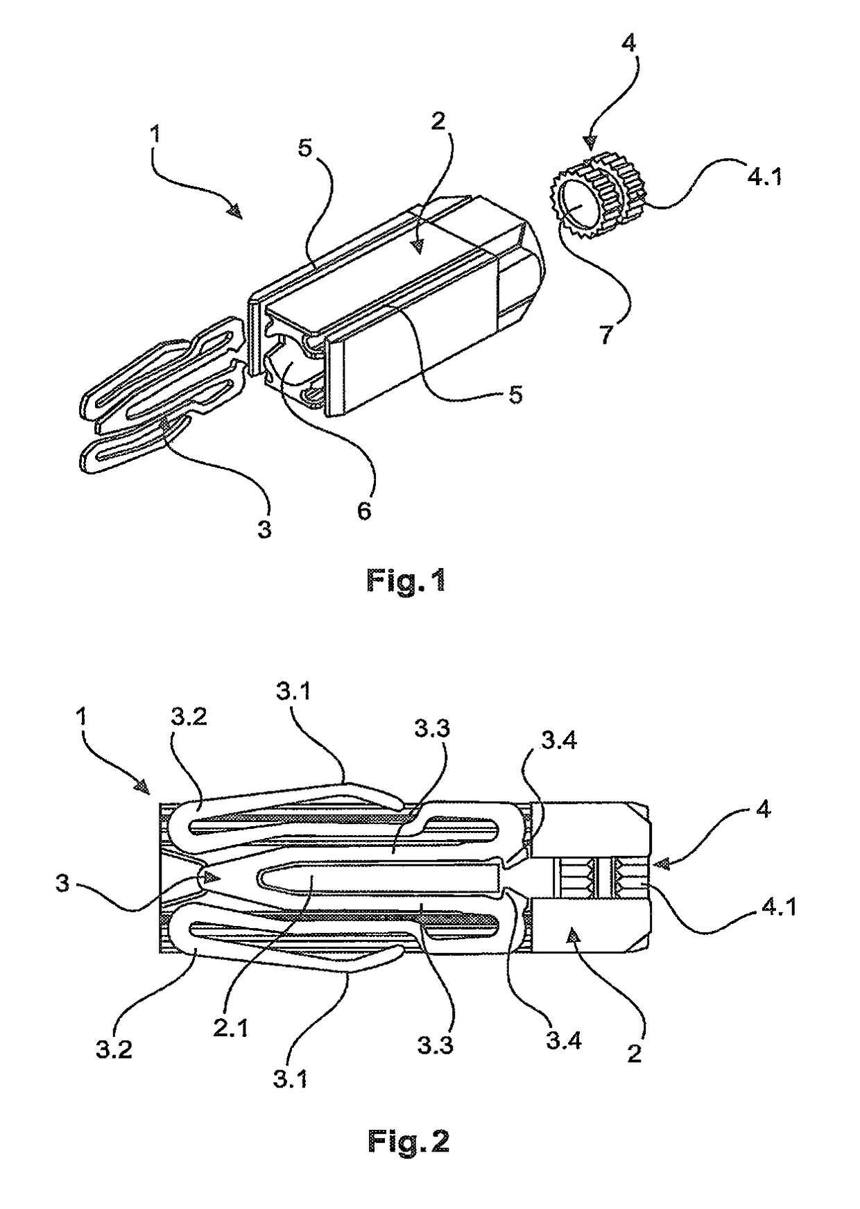
[0022]FIG. 1 illustrates a sliding element 1 in a spatial exploded view. The sliding element 1 comprises a base body 2, a threaded bushing 4 and two contact elements 3. For the sake of the overview, only one of the contact elements 3 is shown.

[0023]The base body 2 of the sliding element 1 has an elongated shape and an approximately square cross section. A through-going opening 6 extends through the entire base body 2. The through-going opening 6 is provided so as to receive a threaded rod 11.

[0024]The threaded bushing 4 is provided on one end of the through-going opening 6, in this case the end illustrated on the right-hand side. The threaded bushing 4 comprises on its outer face a knurling 4.1. The knurling 4.1 is provided so as to press the thread...


PUM


Abstract

A sliding element for electrically contacting conductor paths on two facing printed circuit boards is provided. The sliding element comprises a main body, at least one electrical contact element, and a through-going opening provided for accepting a threaded stud. An internal thread in the through-going opening allows the sliding element to move linearly along the threaded stud when the threaded stud is rotated. By moving the sliding element along the threaded stud, different conductor paths on the printed circuit boards are brought into electrical contact with one another.

Description

BACKGROUNDTechnical Field[0001]This disclosure relates to a sliding element for contacting printed circuit boards.Description of the Related Art[0002]Sliding elements for contacting printed circuit boards are required in order to provide electrical contact between conducting tracks of printed circuit boards that are arranged one above the other and are aligned in parallel with one another. The printed circuit boards are arranged with narrow spacings between one another and comprise a multiplicity of conducting tracks which need to make contact with one another in different ways depending upon the application and the circuitry.[0003]It is possible depending upon the application to connect multiple conducting tracks of printed circuit boards simultaneously by multiple sliding elements. By virtue of displacing (sliding) the sliding elements between the printed circuit boards, it is possible to achieve different positions and thus to close different electrical connections and switching ...

Claims


Application Information

Patent Timeline
Patent Type & Authority Patents(United States)
IPC IPC(8): H01R12/71H01R12/57H01R12/52H01R13/24H01R12/89
CPCH01R12/714H01R12/52H01R12/57H01R13/2435H01R13/24H01R13/245H01R12/89H01R29/00H01R41/00
Inventor PAPE, GUNTER
Owner HARTING ELECTRIC GMBH & CO KG
Why Eureka
Try Eureka