Organic light emitting display device

a light-emitting display and organic technology, applied in semiconductor devices, diodes, electrical devices, etc., can solve the problems of light-emitting display devices, low manufacturing cost, fast response time, etc., and achieve the effect of reducing or preventing the peeled color filter

Active Publication Date: 2019-02-19
LG DISPLAY CO LTD
View PDF8 Cites 0 Cited by
  • Summary
  • Abstract
  • Description
  • Claims
  • Application Information

AI Technical Summary

Benefits of technology

[0017]An aspect of the present disclosure is directed to provide an organic light emitting display device which has a pixel structure where an anode electrode is spaced apart from, by a certain distance, a contact hole for connecting the anode electrode to a TFT, thereby solving a problem of the partial detachment of the anode electrode which occurs in a high resolution model.
[0018]Another aspect of the present disclosure is directed to provide an organic light emitting display device in which color filters are arranged in a stripe type extending along a plurality of subpixels when a pixel structure of a high resolution model is applied, thereby reducing or preventing the color filters from being peeled.

Problems solved by technology

Furthermore, the organic light emitting display devices are driven with a low direct current (DC) voltage, have a fast response time, and are low in manufacturing cost.
On the other hand, there is a limitation in decreasing an area of the contact hole CNT, and thus, a constant area of the contact hole CNT in each subpixel P is maintained.

Method used


Image

  • Organic light emitting display device
  • Organic light emitting display device
  • Organic light emitting display device

Examples


first embodiment

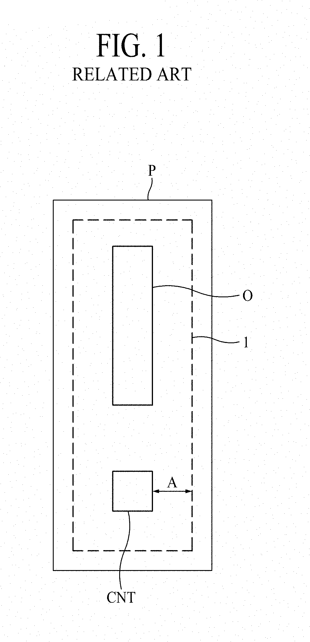
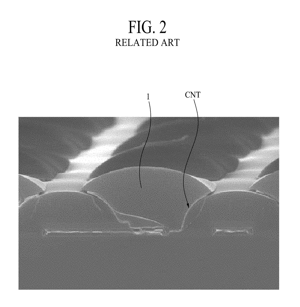
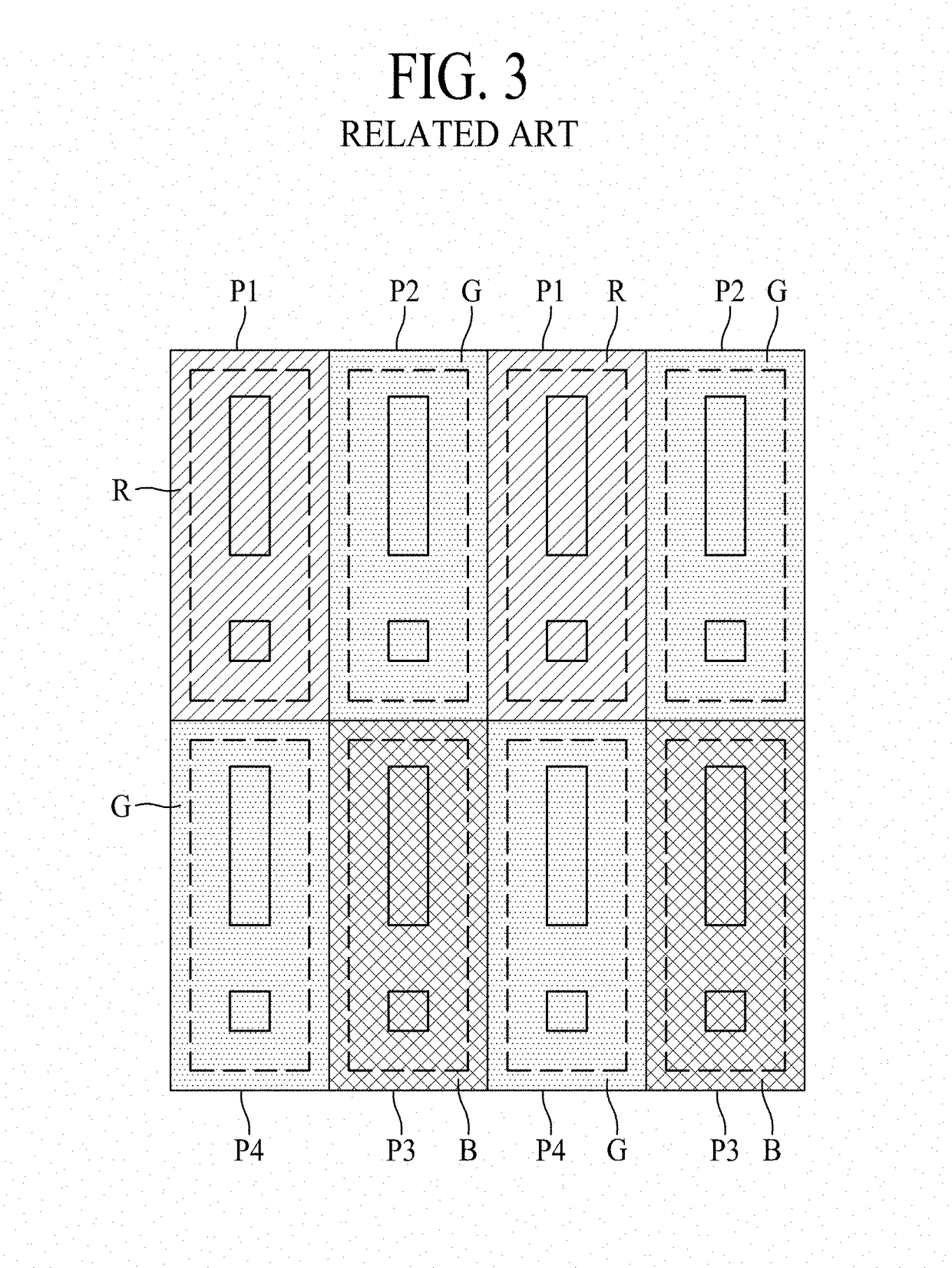
[0119]That is, as illustrated in FIG. 8A, in the organic light emitting display device according to the present disclosure, the first color filter R and the second color filter G may be provided as a stripe type which extends along the first axis direction (the X axis direction), thereby solving a problem where color filters are peeled as in the related art organic light emitting display device illustrated in FIG. 3. However, even in this case, since the third color filter B is disposed as an island type, the third color filter B might peel away.

second embodiment

[0120]In order to solve such a problem, as illustrated in FIG. 8B, in an organic light emitting display device according to the present disclosure, the third subpixel P3 and the fourth subpixel P4 may be provided as the same type as that of each of the second subpixel P2 and the first subpixel P1.

[0121]In detail, the third subpixel P3 may include the third contact hole CH3 and a third anode electrode 182 which are disposed identically to the second contact hole CH2 and the second anode electrode 181 included in the second subpixel P2. That is, when the third contact hole CH3 and the third anode electrode 182 of the third subpixel P3 are horizontally moved with respect to an X-Y plane, the third contact hole CH3 and the third anode electrode 182 of the third subpixel P3 may fully overlap the second contact hole CH2 and the second anode electrode 181 of the second subpixel P2.

[0122]Moreover, the fourth subpixel P4 may include the fourth contact hole CH4 and a fourth anode electrode 18...


PUM


Abstract

Disclosed is an organic light emitting display device for reducing or preventing anodes from being partially detached or torn in high resolution models. The organic light emitting display device includes a substrate including first and second subpixels disposed adjacent to each other in a first axis direction, a first anode electrode provided in the first subpixel and connected to a first TFT of the first subpixel through a first contact hole, and a second anode electrode provided in the second subpixel and connected to a second TFT of the second subpixel through a second contact hole. The first and second contact holes are disposed in a diagonal direction, the first anode electrode protrudes from the first contact hole in a direction toward the second subpixel, and the second anode electrode protrudes from the second contact hole in a direction toward the first subpixel. Accordingly, partial detachment of anode electrodes is reduced, or in some cases, prevented.

Description

CROSS-REFERENCE TO RELATED APPLICATIONS[0001]This application claims the benefit of the Korean Patent Application No. 10-2016-0161912 filed on Nov. 30, 2016, which is hereby incorporated by reference as if fully set forth herein.BACKGROUNDTechnical Field[0002]The present disclosure relates to an organic light emitting display device, and particularly, to an organic light emitting display device for a high resolution model.Description of the Related Art[0003]With the advancement of information-oriented society, various requirements for display devices for displaying an image are increasing. Therefore, various display devices such as liquid crystal display (LCD) devices, plasma display panel (PDP) devices, organic light emitting display devices, etc. are being used recently.[0004]As a type of display device, organic light emitting display devices are self-emitting display devices and are better in viewing angle and contrast ratio than LCD devices. Also, since the organic light emittin...

Claims


Application Information

Patent Timeline
Patent Type & Authority Patents(United States)
IPC IPC(8): H01L27/32
CPCH01L27/3248H01L27/322H01L27/3262H01L27/3246H01L27/3211H10K59/123H10K59/131H10K50/813H10K59/38H10K59/121H10K59/122H10K59/351H10K59/35H10K59/1213
Inventor KIM, JONGSUNGKIM, HO-JIN
Owner LG DISPLAY CO LTD
Why Eureka
Try Eureka