Stacked pixel structures

a pixel structure and pixel structure technology, applied in the field of physical pixel structures in a display, can solve the problems of oled display, large control circuit size, and limited circuit size reduction, and achieve the effect of improving performance control circuits and increasing pixel resolution

Active Publication Date: 2019-06-25
X DISPLAY CO TECH LTD
View PDF167 Cites 5 Cited by
  • Summary
  • Abstract
  • Description
  • Claims
  • Application Information

AI Technical Summary

Benefits of technology

[0012]The present invention provides, inter alia, an inorganic LED display having increased pixel resolution and improved performance control circuits, for example monocrystalline silicon circuits. In certain embodiments, structures of the present invention can be made using micro-transfer printing, enabling the use of micro-LEDs and micro-controllers having lateral dimensions less than or equal to 100, 50, 25, 15, 10, 5, or 3 microns.

Problems solved by technology

However, this size reduction increases manufacturing costs and there are limits to the reduction in size of the circuits, especially in flat-panel displays that rely on layers of amorphous silicon or polysilicon to form the circuits.
Organic light-emitting diode (OLED) displays typically require larger and more complex control circuits than LCDs.
For both of these technologies, control circuits are implemented in thin-film layers of silicon provided over the flat-panel display substrate; as the size of the display substrate increases so does the cost of providing high-quality silicon over the substrate.
It is difficult, therefore to construct a high-resolution iLED display.

Method used


Image

  • Stacked pixel structures
  • Stacked pixel structures
  • Stacked pixel structures

Examples


Embodiment Construction

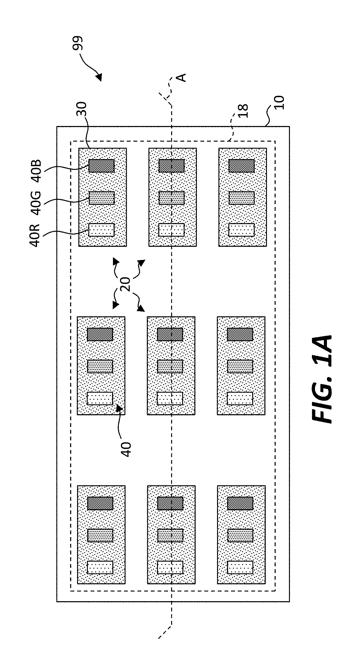
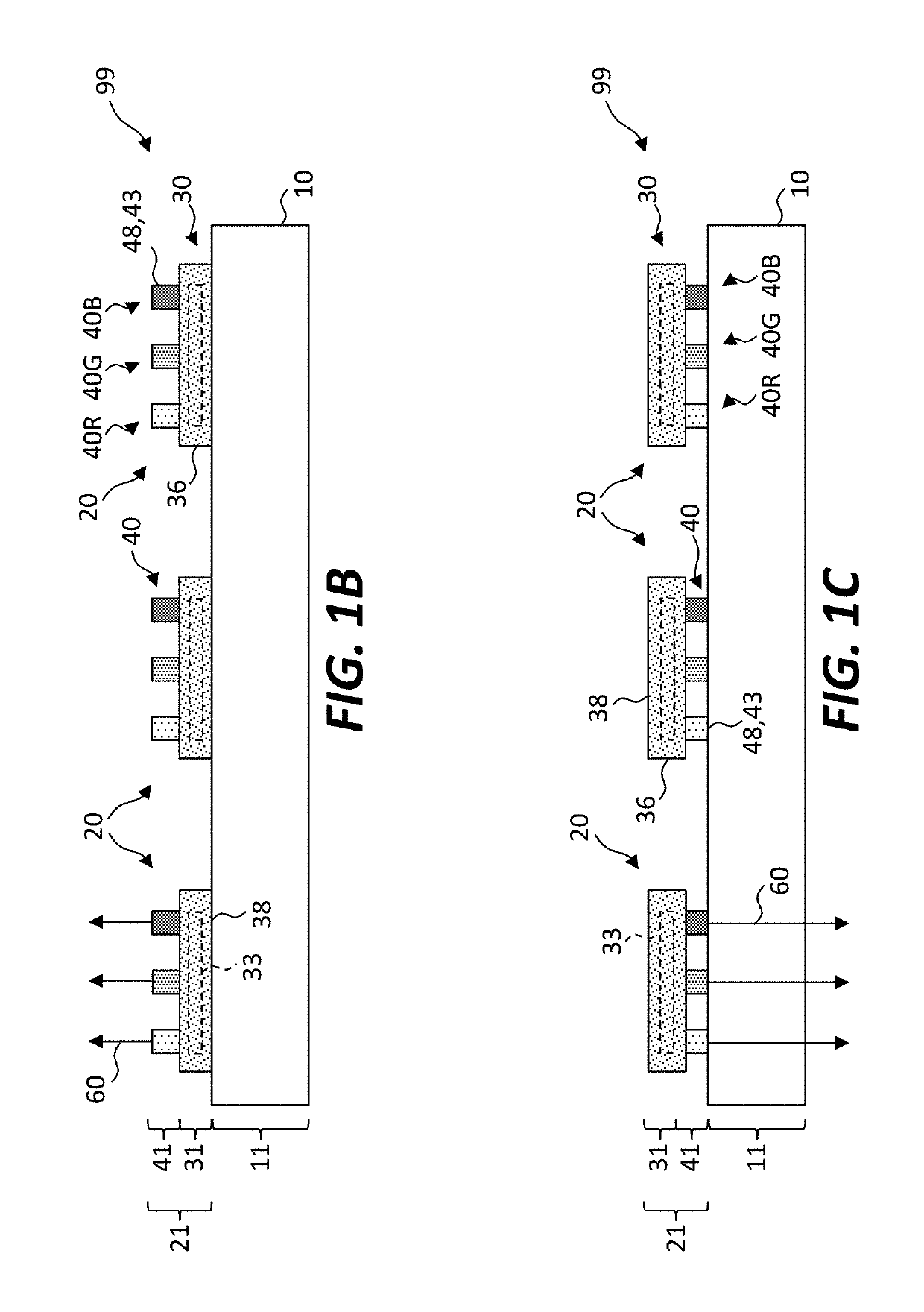
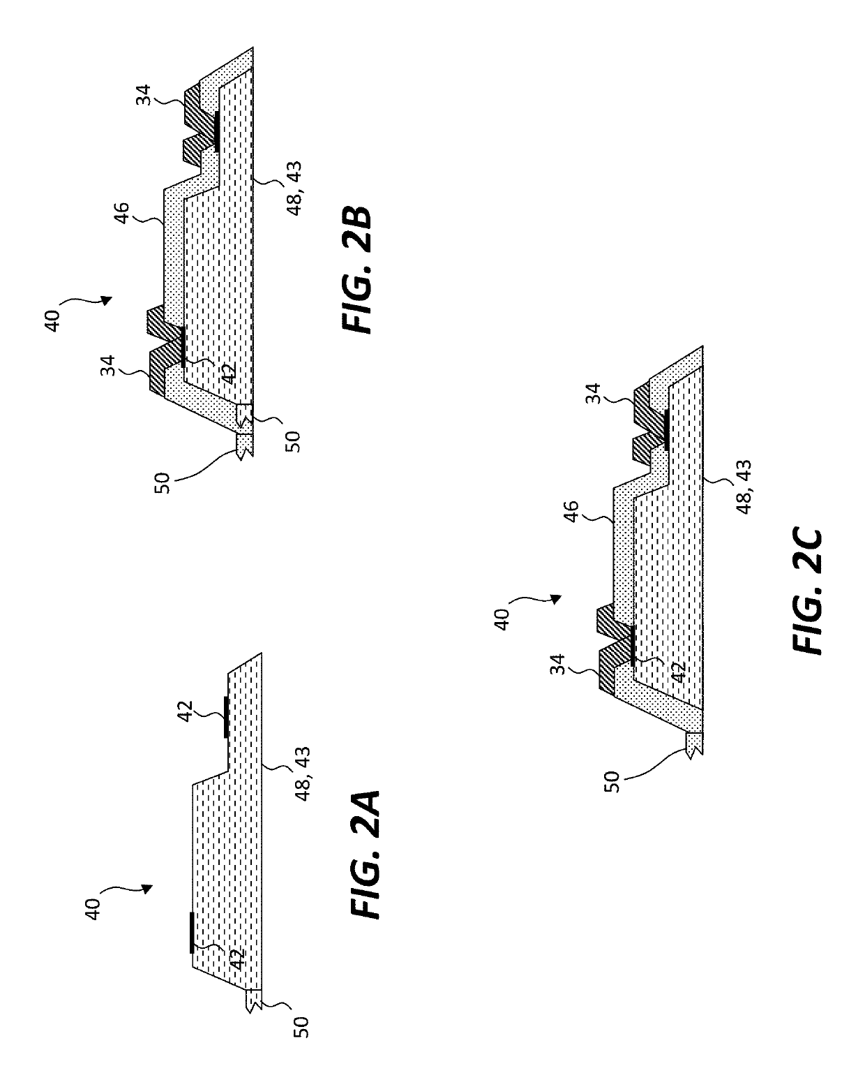
[0053]Certain embodiments of the present invention provide an integrated pixel structure for inorganic light-emitting diodes (iLEDs) pixels in flat-panel displays that have increased resolution and improved performance. Micro-transfer printed pixel control circuits made in monocrystalline silicon, such as CMOS, can provide higher-performance in less space over a display substrate and micro-transfer printed micro-iLEDs can provide increased color saturation, lifetime, and efficiency in a flat-panel display. According to certain embodiments of the present invention, the iLEDs and the pixel control circuits have different, separate, independent, and distinct substrates and are provided in different layers over the same area of a display substrate, thereby reducing the pixel area over the display substrate and facilitating increased display resolution.

[0054]Referring to the plan view schematic illustrations of FIG. 1A and the cross section schematic illustration of FIGS. 1B and 1C taken...


PUM


Abstract

A micro-transfer printed high-resolution inorganic light-emitting diode (iLED) display includes a display substrate and a plurality of pixels disposed over the display substrate, each pixel including a pixel controller disposed or formed in or on a pixel substrate and controlling one or more iLEDs disposed or formed in or on respective iLED substrates. The one or more iLEDs are disposed above or below the pixel controller in a separate layer from the pixel controller. The display substrate, the iLED substrate(s), and the pixel substrate are all separate, independent and distinct, and the one or more iLEDs and pixel controller are each separate devices.

Description

PRIORITY APPLICATION[0001]This application claims the benefit of U.S. Provisional Patent Application No. 62 / 450,866, filed Jan. 26, 2017, entitled Stacked Pixel Structure, the disclosure of which is incorporated by reference herein in its entirety.FIELD OF THE INVENTION[0002]The present invention relates generally to physical pixel structures in a display and in particular to structures with stacked inorganic light emitters and pixel controllers.BACKGROUND OF THE INVENTION[0003]Flat-panel displays have an array of pixels distributed in a display viewing area over a display substrate. The pixels are electrically controlled using matrix addressing with the intersection of row and column wires on the substrate defining pixel locations and from which rows of pixels in the array are sequentially provided with control signals. Passive-matrix control relies on row and column controllers external to the display viewing area to sequentially enable rows of pixels to emit light, so that only o...

Claims


Application Information

Patent Timeline
Patent Type & Authority Patents(United States)
IPC IPC(8): H01L27/16H01L27/13H01L27/07H01L33/00G09G3/20G09G3/32H01L25/13H01L33/62H01L25/16H01L25/075
CPCH01L25/167G09G3/2088G09G3/32H01L25/0753H01L33/0079H01L25/13H01L2933/0066H01L33/62H01L2224/18H01L33/0093
Inventor COK, RONALD S.RAYMOND, BROOKBOWER, CHRISTOPHER ANDREW
Owner X DISPLAY CO TECH LTD
Why Eureka
Try Eureka