Top-emitting OLED and a manufacturing method thereof

a technology of organic light-emitting diodes and manufacturing methods, which is applied in the field of display, can solve the problems that the beoled device cannot meet the requirement of high-resolution display in the future, and achieve the effect of improving the cathode transmittance of the teoled

Active Publication Date: 2019-07-23
TCL CHINA STAR OPTOELECTRONICS TECH CO LTD
View PDF7 Cites 0 Cited by
  • Summary
  • Abstract
  • Description
  • Claims
  • Application Information

AI Technical Summary

Benefits of technology

[0005]The present invention provides a Top-Emitting Organic Light Emitting Diode (TEOLED) and a manufacturing method thereof. It can effectively improve cathode transmittance of the TEOLED and modulate the coupling output of lights with multiple wavelengths.
[0009]The benefit of the present invention is that the nano particles of high refraction index are prepared on the cathode layer to form the scattering layer, distinguishing from the conventional art. It can effectively improve cathode transmittance of the TEOLED and modulate the coupling output of lights with multiple wavelengths.

Problems solved by technology

With resolution increasing, aperture ratio can be lower so BEOLED device cannot meet requirement of future high resolution displaying.

Method used


Image

  • Top-emitting OLED and a manufacturing method thereof
  • Top-emitting OLED and a manufacturing method thereof

Examples


Embodiment Construction

[0015]To better and concisely explain the disclosure, the same name or the same reference number given or appeared in different paragraphs or figures along the specification should has the same or equivalent meanings while it is once defined anywhere of the disclosure. In the case of no conflict, the following embodiments and the features thereof can be combined with each other.

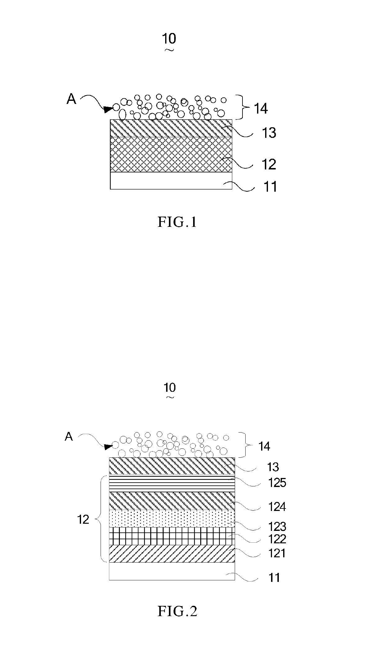
[0016]Referring FIGS. 1-2, FIG. 1 is a schematic view of a Top-Emitting Organic Light Emitting Diode (TEOLED) in accordance with an embodiment of the present invention, and FIG. 2 is a schematic view of a TEOLED in accordance with another embodiment of the present invention. The TEOLED 10 includes a substrate 11, a stack structure 12, a cathode layer 13, and a light-scattering layer 14.

[0017]The substrate 11 can include transparent material. Specifically, it can be a substrate of any type such as glass, ceramic substrate, or transparent plastic. The present invention is not limited.

[0018]The stack structure 1...


PUM

PropertyMeasurementUnit
diameteraaaaaaaaaa
transparencyaaaaaaaaaa
thicknessaaaaaaaaaa

Abstract

The present invention provides a Top-Emitting Organic Light Emitting Diode (TEOLED) and a manufacturing method thereof. The TEOLED includes a substrate; a stack structure on the substrate; a cathode layer covering the stack structure; and a light-scattering layer composed of nano particles and including a concave and convex structure. The present invention can effectively improve cathode transmittance of the TEOLED and modulate the coupling output of lights with multiple wavelengths.

Description

BACKGROUND[0001]Technical Field[0002]The present invention relates to display field, and more particularly, to a Top-Emitting Organic Light Emitting Diode (TEOLED) and a manufacturing method thereof.[0003]Description of Related Art[0004]Organic Light Emitting Diode (OLED) has advantage such as high brightness, self-luminous, rapid response, and low forward voltage and has become new technology of display field. The type of the OLED device can be divided to two structures according to difference of emitting direction, top-emitting (TE) OLED and bottom-emitting (BE) OLED. Active-matrix organic light-emitting diode (AM-OLED) is one of research focus for future large size and high resolution organic display device. It requires that the OLDE device coordinates with Thin Film Transistor (TFT). BEOLED device can only emit light from the bottom and aperture ratio is low because of bottom driving circuit. With resolution increasing, aperture ratio can be lower so BEOLED device cannot meet re...

Claims


Application Information

Patent Timeline
Patent Type & Authority Patents(United States)
IPC IPC(8): H01L29/08H01L51/52H01L51/56H01L21/02H01L51/50
CPCH01L51/5268H01L21/02601H01L51/5056H01L51/5072H01L51/56H01L51/5271H01L2251/5369H01L51/5203H01L2251/5315H10K50/00H10K50/854H10K71/00H10K2102/3026H10K2102/331H10K50/15H10K50/16H10K50/856H10K50/805
Inventor SHI, TING
Owner TCL CHINA STAR OPTOELECTRONICS TECH CO LTD
Why Eureka
Try Eureka