
A flexible organic light-emitting device and its preparation method and display device

An organic light-emitting device, flexible technology, applied in the direction of organic semiconductor devices, semiconductor/solid-state device manufacturing, electric solid-state devices, etc., can solve problems such as difficulty in light extraction, reduce device efficiency, etc., to increase light extraction rate, eliminate total reflection, improve The effect of efficiency

Active Publication Date: 2022-07-19
JILIN OPTICAL & ELECTRONICS MATERIALS
View PDF7 Cites 0 Cited by
  • Summary
  • Abstract
  • Description
  • Claims
  • Application Information

AI Technical Summary

Problems solved by technology

Since the current thin-film packaging method uses SiN material with low refractive index, the OLED optical path has a certain degree of total reflection at the interface between the light extraction layer and the thin-film packaging, which makes it difficult to extract light and ultimately reduces the efficiency of the device.

Method used


Image

  • A flexible organic light-emitting device and its preparation method and display device
  • A flexible organic light-emitting device and its preparation method and display device
  • A flexible organic light-emitting device and its preparation method and display device

Examples


Embodiment 1

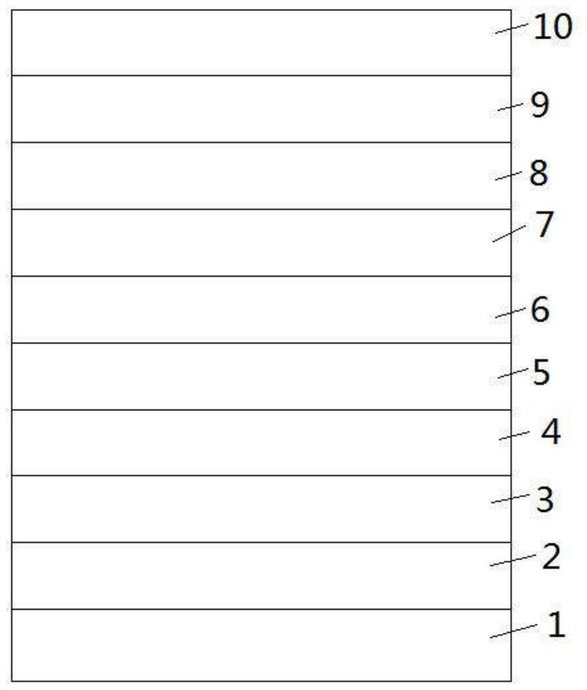
[0050] as attached figure 1 As shown, this embodiment provides a flexible organic light-emitting device, and its specific preparation method includes the following steps:

[0051] S1. Use transparent glass with ITO on the surface as the substrate, then ultrasonically clean with deionized water, acetone, and ethanol for 15 minutes each, and then treat in a plasma cleaner for 2 minutes to obtain the first electrode 1 .

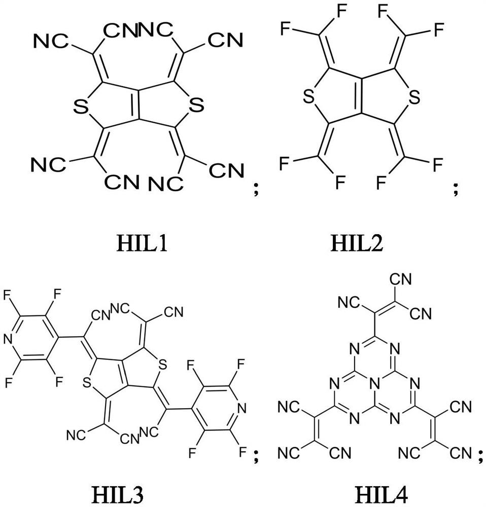
[0052] S2 , on the washed first electrode 1 , a hole injection material HIL1 is prepared by vacuum evaporation, with a thickness of 10 nm, as the hole injection layer 2 .

[0053] S3 . On the hole injection layer 2 , a hole transport material HTL1 is prepared by vacuum evaporation with a thickness of 125 nm as the hole transport layer 3 .

[0054] S4 , on the hole transport layer 3 , the electron blocking material EBL1 is prepared by vacuum evaporation with a thickness of 5 nm, which is used as the electron blocking layer 4 .

[0055] S5 , on the electron bloc...

Embodiment 2

[0061] as attached figure 1 As shown, this embodiment provides a flexible organic light-emitting device, and its specific preparation method includes the following steps:

[0062] S1. Use transparent glass with ITO on the surface as the substrate, then ultrasonically clean with deionized water, acetone, and ethanol for 15 minutes each, and then treat in a plasma cleaner for 2 minutes to obtain the first electrode 1 .

[0063] S2 , on the washed first electrode 1 , a hole injection material HIL1 is prepared by vacuum evaporation, with a thickness of 10 nm, as the hole injection layer 2 .

[0064] S3 . On the hole injection layer 2 , a hole transport material HTL1 is prepared by vacuum evaporation with a thickness of 125 nm as the hole transport layer 3 .

[0065] S4 , on the hole transport layer 3 , the electron blocking material EBL1 is prepared by vacuum evaporation with a thickness of 5 nm, which is used as the electron blocking layer 4 .

[0066] S5 , on the electron bloc...

Embodiment 3

[0072] as attached figure 1 As shown, this embodiment provides a flexible organic light-emitting device, and its specific preparation method includes the following steps:

[0073] S1. Use transparent glass with ITO on the surface as the substrate, then ultrasonically clean with deionized water, acetone, and ethanol for 15 minutes each, and then treat in a plasma cleaner for 2 minutes to obtain the first electrode 1 .

[0074] S2 , on the washed first electrode 1 , a hole injection material HIL1 is prepared by vacuum evaporation, with a thickness of 10 nm, as the hole injection layer 2 .

[0075] S3 . On the hole injection layer 2 , a hole transport material HTL1 is prepared by vacuum evaporation with a thickness of 125 nm as the hole transport layer 3 .

[0076] S4 , on the hole transport layer 3 , the electron blocking material EBL1 is prepared by vacuum evaporation with a thickness of 5 nm, which is used as the electron blocking layer 4 .

[0077] S5 , on the electron bloc...


PUM

PropertyMeasurementUnit
thicknessaaaaaaaaaa
thicknessaaaaaaaaaa

Abstract

The invention discloses a flexible organic light-emitting device, a preparation method thereof, and a display device, belonging to the technical field of electronic display. The flexible organic light-emitting device sequentially comprises a first electrode, a hole transport region, a light-emitting layer, an electron transport region and a second electrode , wherein a first light extraction layer and a second light extraction layer are arranged on the side of the second electrode away from the electron transport region in sequence; the first light extraction layer includes a first light extraction material; the second light extraction layer The light extraction layer includes a second light extraction material; the refractive index of the first light extraction material is greater than the refractive index of the second light extraction material. The present invention can well solve the problem of "the optical path of the flexible organic light-emitting device has a certain degree of total reflection at the interface between the light extraction layer and the film encapsulation, resulting in difficulty in light extraction" by using the light extraction layer material with high and low refractive index, thereby improving the efficiency of light extraction. Efficiency of flexible organic light-emitting devices.

Description

technical field [0001] The invention relates to the technical field of electronic display, in particular to a flexible organic light-emitting device, a preparation method thereof, and a display device. Background technique [0002] Organic electroluminescence (EL) refers to a luminescence phenomenon in which organic materials directly convert electrical energy into light energy under the action of an electric field. It has the characteristics of self-illumination, bright colors, thin thickness, light weight, fast response speed, wide viewing angle, low driving voltage, resistance to harsh natural conditions, and can be made into flexible panels. It has gradually developed into a new generation of flat panel displays. Advantage technology. [0003] The emergence of flexible OLED devices determines that the current OLED packaging method will change from hard screen packaging to flexible thin film packaging (TFE, Thin Film Encapsulation). Traditional OLED devices use a single-...

Claims


Application Information

Patent Timeline
Patent Type & Authority Patents(China)
IPC IPC(8): H01L51/52H01L51/54H01L51/50H01L51/56H01L27/32
CPCH10K59/10H10K85/656H10K85/6565H10K85/636H10K85/626H10K85/633H10K85/631H10K85/615H10K85/654H10K85/6576H10K85/6574H10K85/6572H10K85/657H10K50/18H10K50/15H10K50/16H10K50/17H10K50/858H10K2102/311H10K71/00
Inventor 邱镇马晓宇王铁李天佑刘长伟王伟哲杨勇
Owner JILIN OPTICAL & ELECTRONICS MATERIALS
Learn More