Printed board

a printed board and board body technology, applied in the field of printed boards, can solve the problems of increasing the speed of signals or equipment sizes, difficult to conform to emi, and higher frequency of power supply noise, and achieve the effect of suppressing emi emissions

Inactive Publication Date: 2019-08-06
NEC CORP
View PDF16 Cites 0 Cited by
  • Summary
  • Abstract
  • Description
  • Claims
  • Application Information

AI Technical Summary

Benefits of technology

[0020]According to the present invention, the printed board capable of suppressing the EMI emissions from the power supply wirings can be disposed.

Problems solved by technology

In recent years, getting larger capacities of information communication equipment leads increases of speed of signals or sizes of equipment and causes higher frequencies of power supply noise or multi-purposing of resonance modes in the inside of the equipment, thus having become hard to conform to EMI regulations such as Voluntary Control Council for Interference by Information Technology Equipment (VCCI).
As described below, while EMI reduction techniques have been proposed, EMI emissions have not been solved.
Although there are some effects for suppressing EMI by arranging the GND via holes, the effects are insufficient to block electromagnetic waves, because a great gap is presence due to the GND wiring shaped in the square ring, which the electromagnetic waves are leaked from the gap.
However, the power supply noise propagates the electromagnetic waves to its circumference through between the power supply and GND as if a transmission path, so that it is hard to fundamentally suppress EMI.

Method used


Image

  • Printed board
  • Printed board
  • Printed board

Examples


first example embodiment

[0036]The first example embodiment of the present invention will be described using FIG. 1 to FIG. 5.

(Description of Configurations)

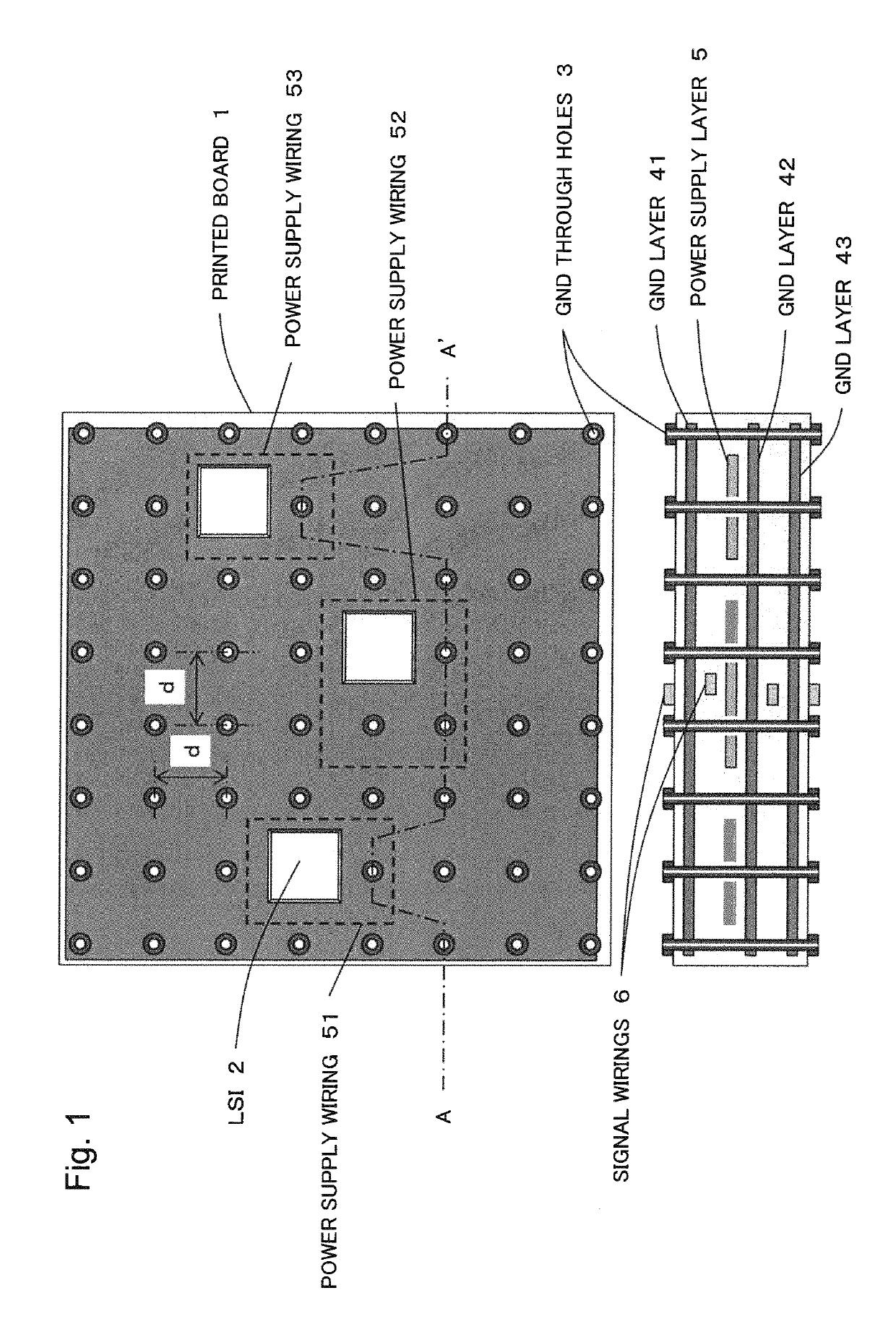
[0037]FIG. 1 is the plan view and the cross-sectional view illustrating a printed board 1 of the first example embodiment of the present invention. The cross-sectional view illustrates a cross section taken along a dashed-dotted line A-A′ in the plan view. For easily understandable, the cross section is presented not by cutting along a straight line, but by taken along a polygonal line so as to pass positions containing the power supply layers. The printed board 1 is a multilayer printed board in which, by putting insulating layers therebetween, power supply layers 5 and signal wirings 6 are formed.

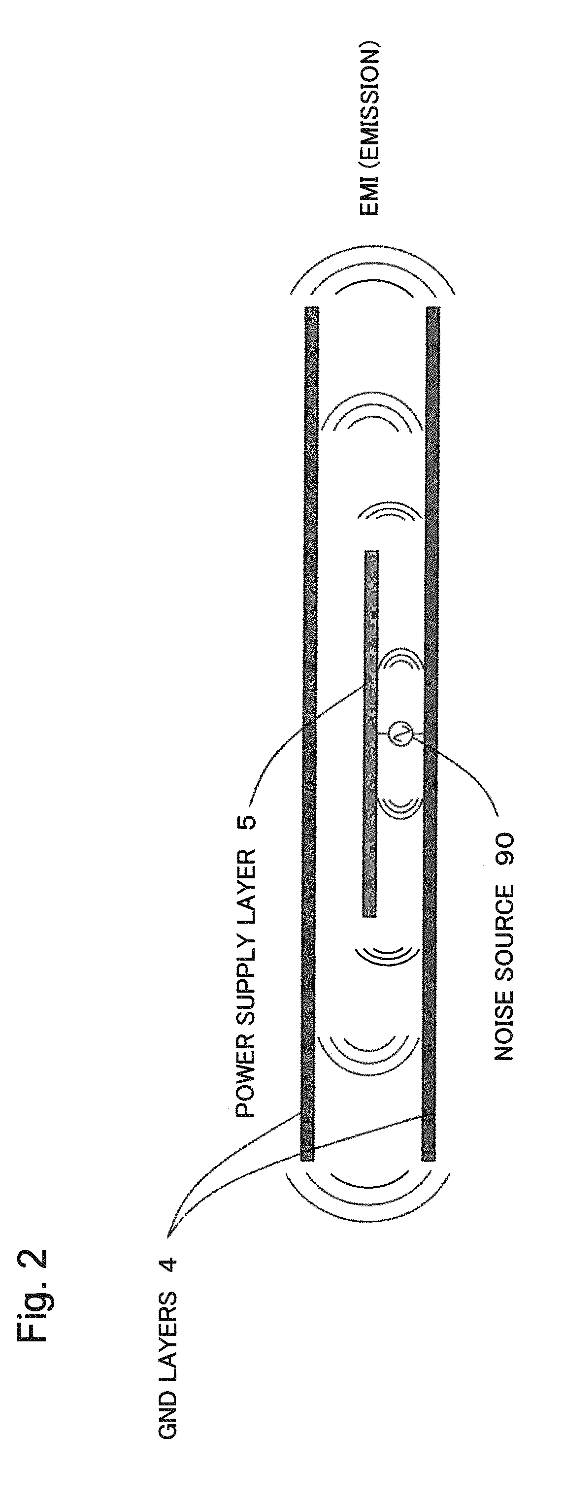
[0038]On at least directly under a component surface (in FIG. 1, one surface side on which LSI 2 is disposed) and directly over a solder surface (the opposite surface side opposite to the component side), GND layers 41, 42, 43 are formed as grounds that are f...

second example embodiment

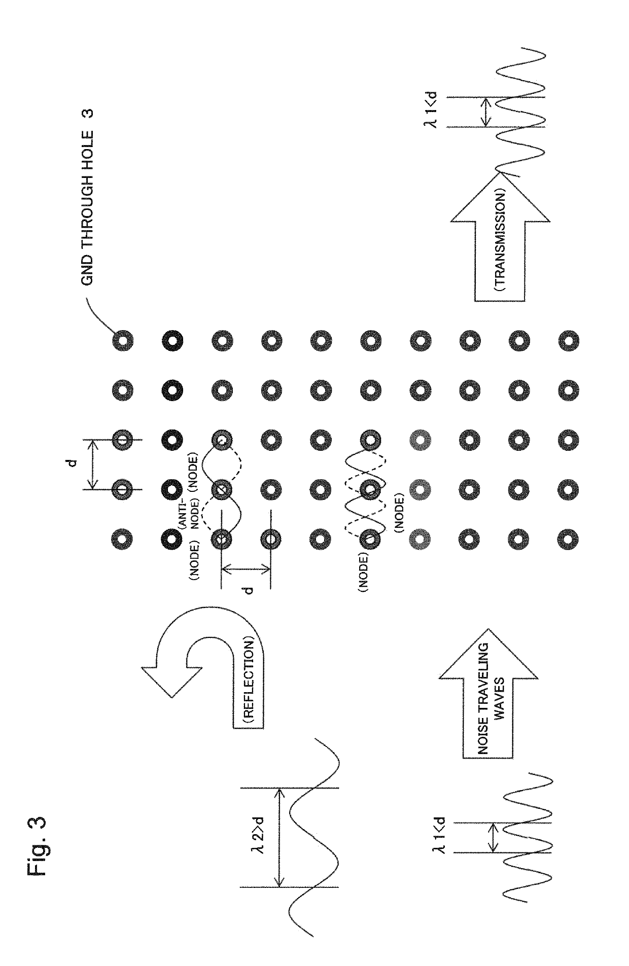
[0054]In the conditions analyzed in FIG. 7, although the only single circuit of the GND through holes 3 is arranged along the periphery of the board, the EMI emissions are generated in the outside of the board 1. An effect for preventing to travel the electromagnetic waves is provided by not arranging the GND through holes 3 on the entire board surface but radially arranging in double circuits, triple circuits, or more thereof on the board.

[0055]FIG. 11 and FIG. 12 are the analysis results of the electric field intensities in the inside and outside of the printed board 1 when the double circuits of the GND through holes 3 are arranged, and the triple circuits thereof are arranged, respectively. In both FIGS. 11 and 12, the EMI emissions to the outside of the board are not observed. FIG. 13 is the results of analyzing the relationship between the frequencies and the electric field intensities measured by the probe, which is positioned at the observation point outside the board, conce...

third example embodiment

[0057]FIG. 14 is the plan view illustrating the third example embodiment of the present invention and the cross-sectional view taken along the B-B′ thereof. In the B-B′ cross sectional view, the IC is omitted. In the first and second example embodiments, the propagations of the power supply noise to the outside of the printed board have been suppressed. In the present example embodiment, the propagations of the power supply noise to circumference of the power supply layers in the board are suppressed.

[0058]In the present example embodiment, the power supply layer, i.e., a power feeding wiring for the IC 54, is in a lower layer than the IC 21 and runs across the printed board 1 along the vertical direction of the plan view. The GND layer 401 and GND layer 402 are formed above and below the power feeding wiring for the IC 54, respectively, and the GND through holes 3 are disposed only around the power feeding wiring for the IC 54, which is the source of the power supply noise. In FIG....


PUM


Abstract

An objective of the present invention is to provide a printed board being capable of suppressing EMI emissions from power supply wirings. To accomplish the objective, a printed board of the present invention includes a plurality of ground layers disposed in a printed board, a power supply layer put between the plurality of the ground layers, and through holes disposed along at least periphery of the printed board and connecting the plurality of the ground layers, wherein the through holes are disposed at intervals according to a wavelength corresponding to a maximum frequency of electromagnetic waves to be suppressed.Further, a printed board of the present invention includes a power supply layer disposed in a printed board and put between ground layers above and below the power supply layers, and a plurality of through holes connecting the ground layers above and below the power supply layers, wherein the plurality of the through holes are disposed at and near the power supply layer and are spaced apart at intervals according to a wavelength corresponding to a maximum frequency of electromagnetic waves to be suppressed.

Description

[0001]This application is a National Stage Entry of PCT / JP2016 / 003168 filed on Jul. 4, 2016, which claims priority from Japanese Patent Application 2015-137091 filed on Jul. 8, 2015, the contents of all of which are incorporated herein by reference, in their entirety.TECHNICAL FIELD[0002]The present invention relates to a printed board, which suppresses electro-magnetic interference (EMI), particularly to a printed board, which suppresses EMI caused by power supply noise.BACKGROUND ART[0003]In recent years, getting larger capacities of information communication equipment leads increases of speed of signals or sizes of equipment and causes higher frequencies of power supply noise or multi-purposing of resonance modes in the inside of the equipment, thus having become hard to conform to EMI regulations such as Voluntary Control Council for Interference by Information Technology Equipment (VCCI).[0004]As described below, while EMI reduction techniques have been proposed, EMI emissions ...

Claims


Application Information

Patent Timeline
Patent Type & Authority Patents(United States)
IPC IPC(8): H05K1/11H05K1/02H05K9/00H05K3/46
CPCH05K1/0216H05K1/0218H05K1/0243H05K1/11H05K9/0064H05K3/46H05K2201/10H05K2201/09309H05K2201/09327H05K2201/09609
Inventor KASHIWAKURA, KAZUHIROUEMURA, AYAKO
Owner NEC CORP
Why Eureka
Try Eureka