Ultrasound sensor and method of manufacturing thereof
a technology of ultrasonic sensors and manufacturing methods, applied in the field of ultrasonic sensors, can solve the problems of difficult use, different piezoelectric materials to be arranged, etc., and achieve the effect of improving transmission performance and reception performan
- Summary
- Abstract
- Description
- Claims
- Application Information
AI Technical Summary
Benefits of technology
Problems solved by technology
Method used
Image

Examples
embodiment 1
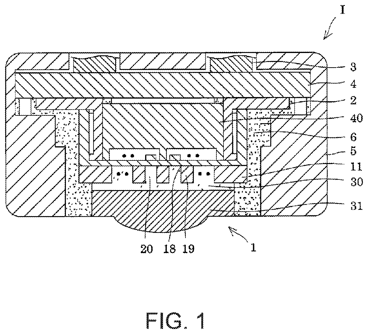
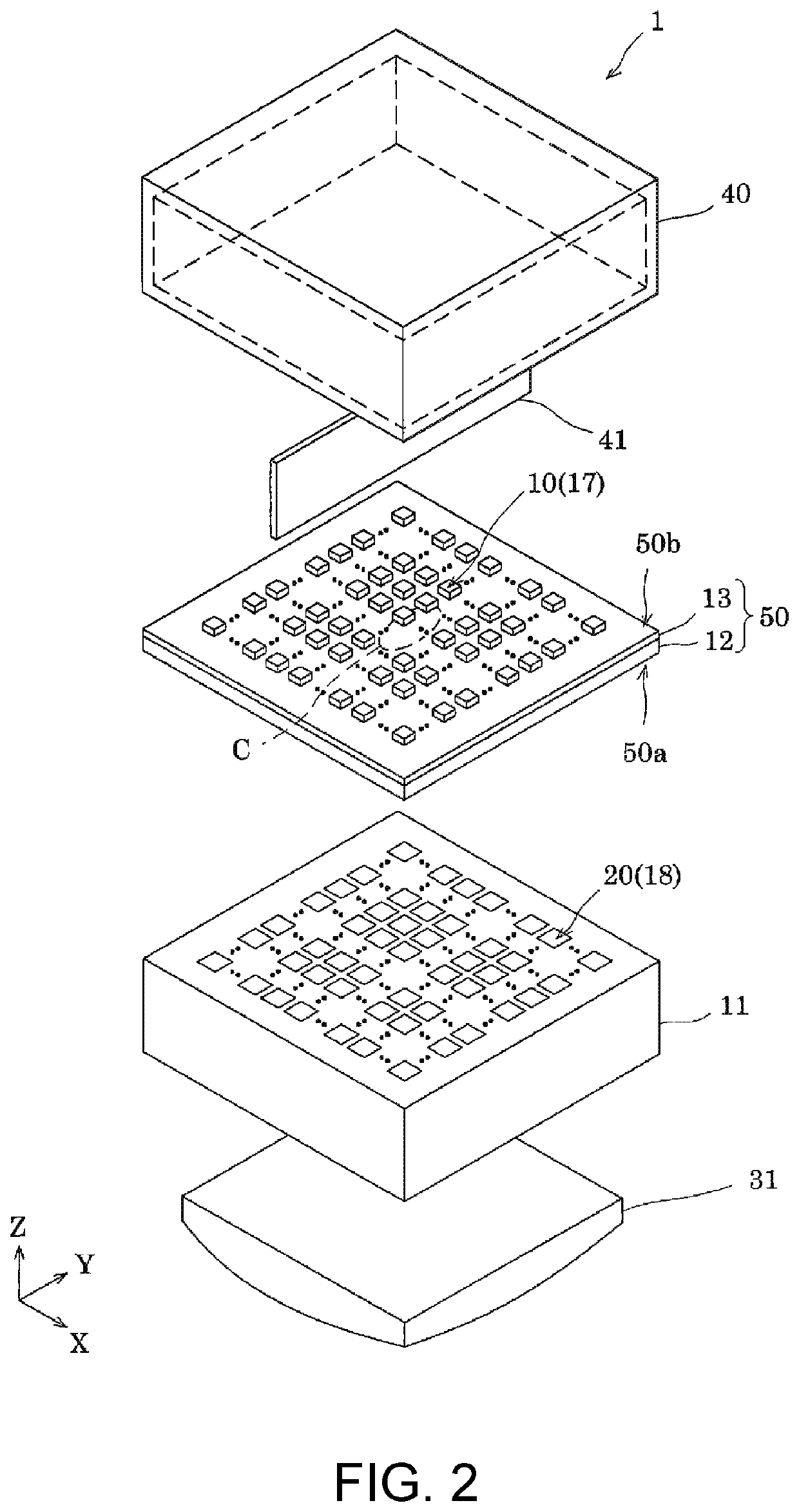
[0039]Ultrasound Device FIG. 1 is a cross-sectional view illustrating a configuration example of an ultrasound device on which the ultrasound sensor according to Embodiment 1 of the invention is mounted. As illustrated in FIG. 1, the ultrasound probe I is formed including a CAV surface type ultrasound sensor 1, a flexible printed substrate (FPC substrate 2) connected to the ultrasound sensor 1, a cable 3 drawn out from an apparatus terminal (not shown), a relay substrate 4 that serves as an intermediate between the FPC substrate 2 and the cable 3, a housing 5 that protects the ultrasound sensor 1, the FPC substrate 2 and the relay substrate 4, and a waterproof resin 6 which fills the space between the housing 5 and the ultrasound sensor 1.
[0040]Ultrasound waves are transmitted from the ultrasound sensor 1. Ultrasound waves reflected from a measurement target are received by the ultrasound sensor 1. Information (such as position and shape) pertaining to the measurement target is dete...
embodiment 2
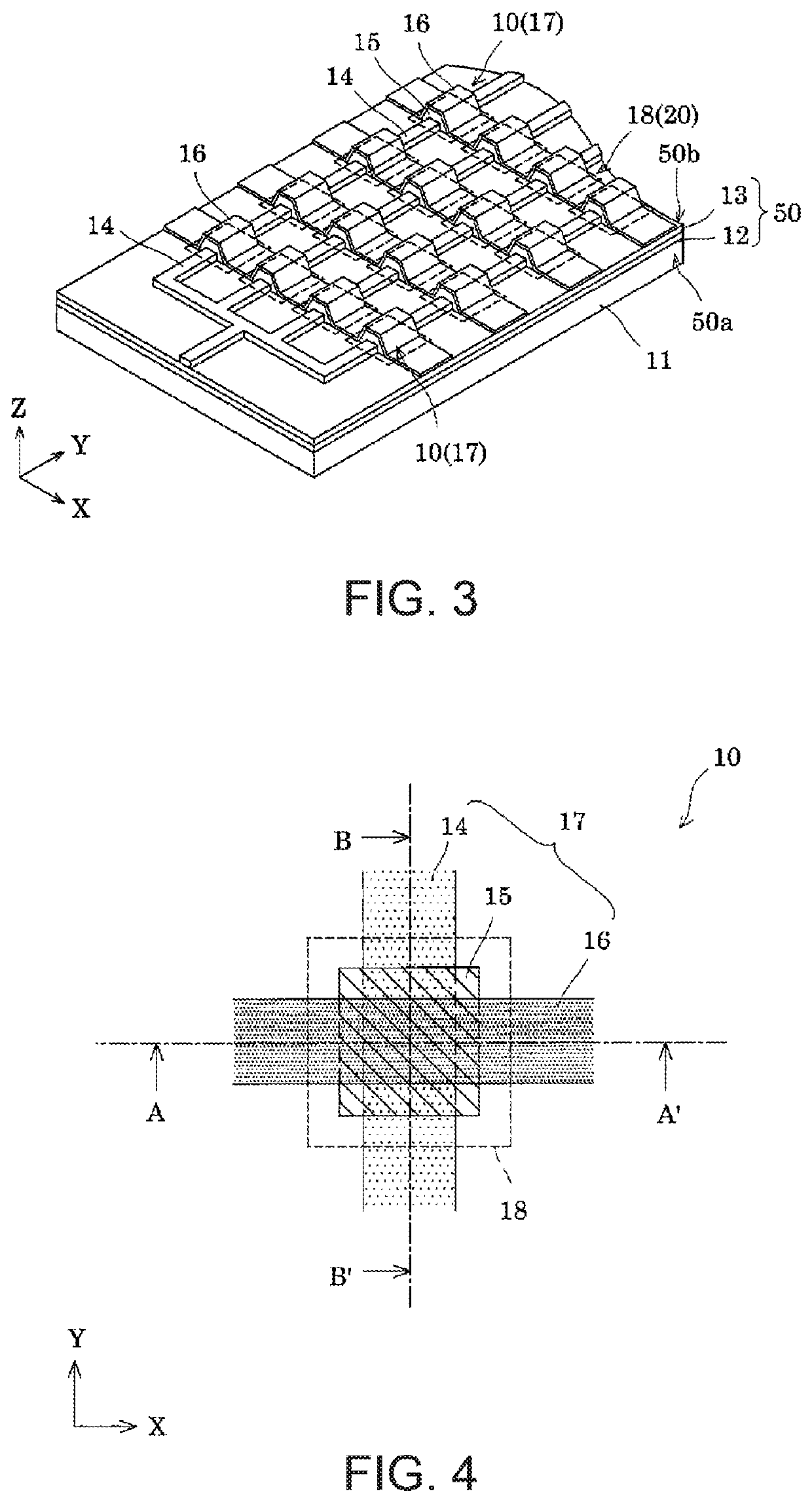
[0075]An ultrasound sensor 1A of Embodiment 2 will be described with reference to one example of the manufacturing method. Each of FIGS. 14 to 19 illustrates each process and includes a plan view and cross-sectional views taken along lines b-b′ and c-c′. In Embodiment 1 stated above, the second electrode 16 is a common electrode, but in Embodiment 2, the first electrode 14 is a common electrode.
[0076]First, as illustrated in FIGS. 14A, 14B and 14C, after forming an elastic film 12 formed of silicon oxide by thermal oxidation or the like of a substrate 11, a zirconium film is formed thereupon, and thermally oxidized at 500 to 1200° C., and an insulator film 13 formed of zirconium oxide is formed. The first electrode 14 is formed on the insulator film 13 by a sputtering method, a deposition method or the like, and patterning carried out so that the first electrode 14 takes a predetermined shape.
[0077]Next, as illustrated in FIGS. 15A, 15B and 15C, the piezoelectric layer 15 is layered...
embodiment 3
[0082]FIGS. 20A, 20B and 20C show an ultrasound sensor 1B of Embodiment 3. In the present embodiment, when patterning the secondary second electrode 16b, the second electrode 16 and a discontinuous electrode 22 which is electrically discontinued from the second electrode 16 are separated by a groove 21 instead of removing unnecessary portion of the second electrode 16. By varying a forming position of the groove 21, the wider second electrode 16A is provided in a center row in the vertical direction, the narrower second electrodes 16B are provided on both sides in the vertical direction, the dedicated transmission piezoelectric element 17A is provided in a center row and the dedicated reception piezoelectric elements 17B are provided on both sides in the vertical direction.
[0083]This process also enables that the dedicated transmission piezoelectric element 17A and the dedicated reception piezoelectric element 17B can be manufactured and transmission performance and reception perfor...
PUM
 Abstract
Description
Claims
Application Information
 - R&D Engineer
- R&D Manager
- IP Professional
- Industry Leading Data Capabilities
- Powerful AI technology
- Patent DNA Extraction
Browse by: Latest US Patents, China's latest patents, Technical Efficacy Thesaurus, Application Domain, Technology Topic.
© 2024 PatSnap. All rights reserved.Legal|Privacy policy|Modern Slavery Act Transparency Statement|Sitemap