
OLED display panel and OLED display device

a display panel and display device technology, applied in the field of liquid crystal display technology, can solve the problems of difficult integration of fingerprint recognition technology into display screens, urgent improvements, and inability to complete fingerprint recognition, and achieve the effect of increasing the screen ratio

Active Publication Date: 2021-07-20
WUHAN CHINA STAR OPTOELECTRONICS SEMICON DISPLAY TECH CO LTD
View PDF9 Cites 0 Cited by
  • Summary
  • Abstract
  • Description
  • Claims
  • Application Information

AI Technical Summary

Benefits of technology

The present patent provides an organic light-emitting diode (OLED) display panel and OLED display device with an increased screen ratio effect. This is achieved by dividing the common electrode layer into a first electrode and multiplexed electrodes. The first electrode serves as the common electrode of a first region, while each multiplexed electrode serves as the fingerprint signal acquisition electrode and the common electrode of a second region. The multiplexed functional line is connected to one of the multiplexed electrodes to detect a capacitance change caused by the electrodes and a finger. Therefore, fingerprints can be acquired and a normal display can be realized in the second region, providing an increased screen ratio effect.

Problems solved by technology

Currently, it is difficult to integrate fingerprint recognition technologies into display screens.
Because a surface of AMOLED is a layer of a metal electrode that would shield a display screen from surface fingerprint information, the display screen cannot receive the fingerprint information, and thus fingerprint recognition cannot be completed.
Therefore, there exist deficiencies for existing technologies, and urgent improvements are needed.

Method used


Image

  • OLED display panel and OLED display device
  • OLED display panel and OLED display device

Examples


Embodiment Construction

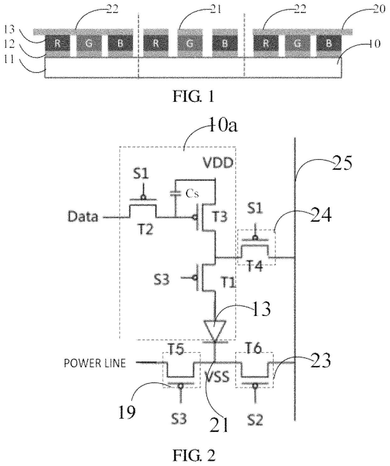
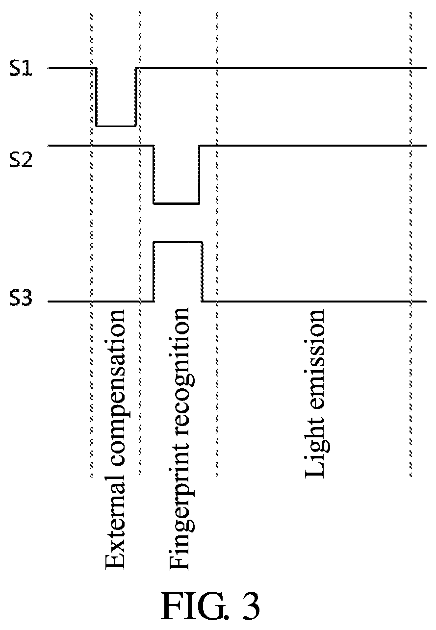
[0049]Embodiments of the present disclosure are described in detail below and examples of the embodiments are illustrated in the accompanying drawings, wherein same or similar labels throughout the present disclosure represent corresponding same or similar elements or corresponding elements having same or similar functions. The description of the embodiments with reference to the accompanying drawings below is exemplary, aims at illustrating the present disclosure, and cannot be considered as limitations to the present disclosure.

[0050]In the description of the present disclosure, it is to be appreciated that orientation or location relationships indicated by terms such as “center”, “longitudinal”, “transverse”, “length”, “width”, “thickness”, “upper”, “lower”, “front”, “back”, “left”, “right”, “vertical”, “horizontal”, “top”, “bottom”, “inside”, “outside”, “clockwise”, “counterclockwise”, etc. are based on orientation or location relationships illustrated in the accompanying drawin...


PUM


Abstract

An organic light-emitting diode (OLED) display panel is provided. The OLED display panel includes a light-emitting layer having a first region and a second region; a common electrode layer including a first electrode and a plurality of multiplexed electrodes insulated from one another, wherein the first electrode is opposite to the first region and each multiplexed electrode is opposite to the second region; and a multiplexed functional line, wherein the multiplexed functional line is electrically connected to one of the plurality of multiplexed electrodes, to detect a capacitance change caused by the one of the plurality of multiplexed electrodes and a finger, and thereby generate a fingerprint signal. An increased screen ratio effect is provided.

Description

FIELD OF INVENTION[0001]The present disclosure relates to a field of liquid crystal display technology, and more particularly to an organic light-emitting diode (OLED) display panel and an OLED display device.BACKGROUND OF INVENTION[0002]Full-screens may greatly enhance screen ratios of cell phones, and are one developmental direction of display screens of cell phones. Integrating fingerprint recognition technologies into cell phone screens can change fingerprint recognition regions that do not emit light into display regions, increasing screen ratios of cell phones. Currently, it is difficult to integrate fingerprint recognition technologies into display screens. There may be differences between image qualities of fingerprint recognition regions and normal display regions in screens. Compensation for pixel display in fingerprint recognition regions is needed, to prevent fingerprint recognition region display from being abnormal. The present disclosure provides an on-screen fingerpr...

Claims


Application Information

Patent Timeline
IPC IPC(8): G06K9/00G09G3/3233
CPCG06K9/0002G09G3/3233G09G2300/0439G09G2300/0819G09G2300/0842G09G3/3225H10K59/00H10K59/12G09G2320/0295G09G2320/045G06V40/1306
Inventor LI, JUN
Owner WUHAN CHINA STAR OPTOELECTRONICS SEMICON DISPLAY TECH CO LTD
Features
  • Generate Ideas
  • Intellectual Property
  • Life Sciences
  • Materials
  • Tech Scout
  • Unparalleled Data Quality
  • Higher Quality Content
  • 60% Fewer Hallucinations
Learn More