Driving circuit for display panel and high voltage tolerant circuit

a driving circuit and high voltage tolerant technology, applied in the direction of electronic switching, pulse technique, instruments, etc., can solve the problem that the solution cannot meet the high standard of liquid crystal display

Active Publication Date: 2022-04-26
SITRONIX TECH CORP
View PDF15 Cites 0 Cited by
  • Summary
  • Abstract
  • Description
  • Claims
  • Application Information

AI Technical Summary

Benefits of technology

[0006]An objective of the present invention is to provide a driving circuit for display panel, which uses power circuits with different driving capabilities for controlling the voltage levels of the gate signals not mutually interference.

Problems solved by technology

Unfortunately, the solution cannot meet the high standard for liquid crystal displays.

Method used


Image

  • Driving circuit for display panel and high voltage tolerant circuit
  • Driving circuit for display panel and high voltage tolerant circuit
  • Driving circuit for display panel and high voltage tolerant circuit

Examples


first embodiment

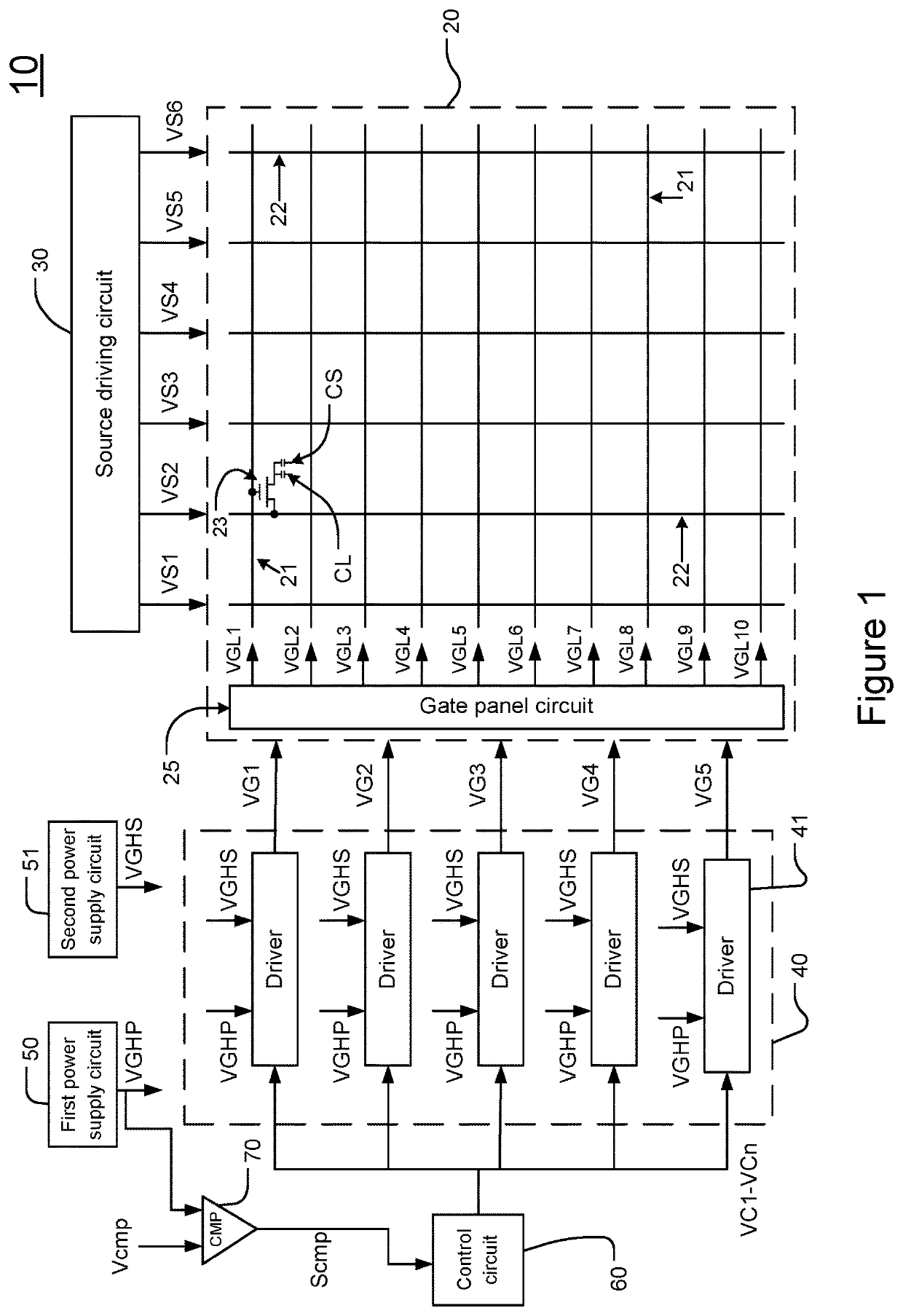
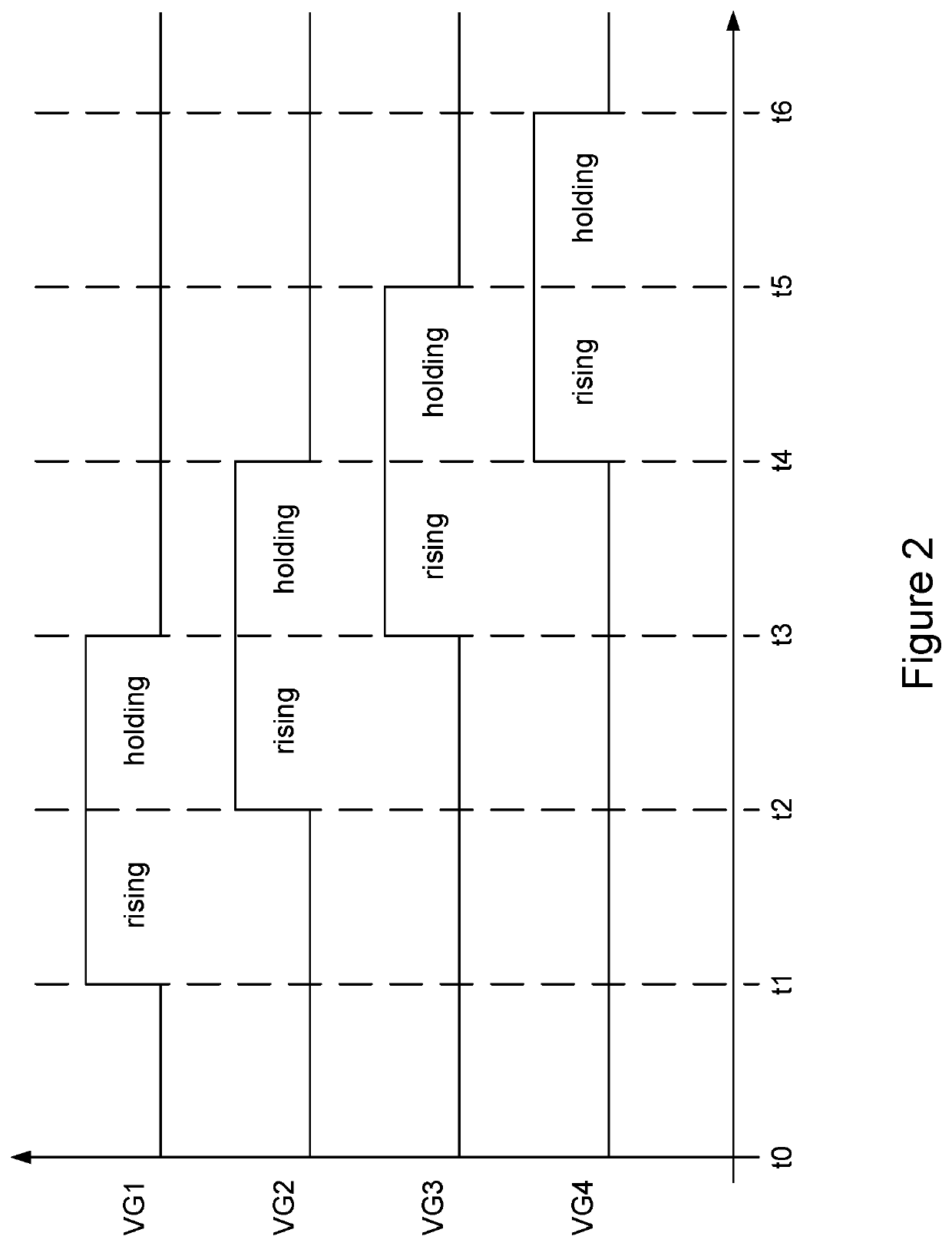
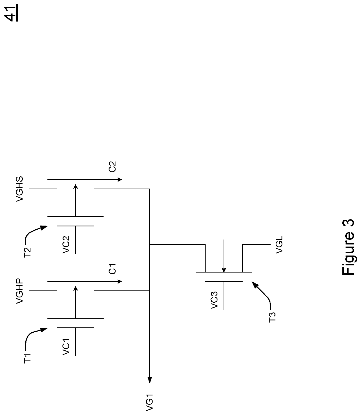
[0025]Please refer to FIG. 3, which shows a circuit diagram of the driver according to the present invention. As shown in the figure, the driver 41 includes a plurality of transistors T1, T2, T3. An input terminal of the transistor T1 is coupled to the first power supply circuit 50 and receives the first supply voltage VGHP. The input terminal of the transistor T1 is a first power supply input terminal of the driver 41. A control terminal of the transistor T1 is coupled to the control circuit 60 for receiving the control signal VC1. An output terminal of the transistor T1 is coupled to an output terminal of the driver 41. After the control circuit 60 outputs the control signal VC1 and controls the transistor T1 to turn on, the transistor T1 transmits the first supply voltage VGHP to the output terminal of the driver 41 for rising the voltage level of the gate signal VG1 to the voltage level of the first supply voltage VGHP in the voltage rising period rising. The input and output te...

second embodiment

[0030]Please refer to FIG. 4, which shows a circuit diagram of the driver according to the present invention. As shown in the figure, to save the power consumption of the gate signal VG1 in the voltage rising period rising, the driver 41 can include a precharge circuit 42, which includes a high voltage device such as a high voltage tolerant transistor T4. The precharge circuit 42 is coupled to the output terminal of the driver 41 for outputting a precharge voltage to the output terminal of the driver 41. Thereby, the gate signal VG1 can be precharged to the voltage level of the precharge voltage before being charged to the voltage level of the first supply voltage VGHP. The embodiment in FIG. 4 includes a third power supply circuit 52, which is capable of outputting precharge voltages with different levels, namely, a first precharge voltage V1 and a second precharge voltage V2 in the embodiment in FIG. 4. The third power supply circuit 52 receives and outputs the first precharge vol...

third embodiment

[0032]Please refer to FIG. 5, which shows a circuit diagram of the driver according to the present invention. As shown in the figure, the precharge circuit 43 in the embodiment in FIG. 5 replaces the precharge circuit 42 in the embodiment in FIG. 4. The difference therebetween is that the precharge circuit 43 in FIG. 5 includes a plurality of transistors. The gate across the body of the plurality of transistors can tolerate medium voltages, while the source across the drain can tolerate high voltages. Thereby, the present invention can be applied to applications requiring tolerance of high voltages. The precharge circuit 42 in FIG. 4 includes one or more high voltage tolerant transistor T4. The precharge circuit 43 includes a plurality of transistors T5, T6, T7, T8, D1. The transistors T5, T6, D1, T7, T8 are a first switching device, a second switching device, a control device, a third switching device, and a fourth switching device of the precharge circuit 43. Thereby, the first sw...


PUM


Abstract

A driving circuit for display panel is provided. Wherein, a first and a second power supply circuits produce a first and a second supply voltages. The electric charge provided by the second power supply circuit is less than that provided by the first power supply circuit. A plurality of drivers include a plurality of first power input terminals and a plurality of second power input terminals. The first power input terminals are coupled to the first power supply circuit and receives the first supply voltage. The second power input terminals are coupled to the second power supply circuit and receives the second supply voltage. The drivers increase the voltage levels of a plurality of gate signals in a voltage rising period according to the first supply voltage. The drivers hold the voltage levels of gate signals in a voltage holding period according to the second supply voltage.

Description

FIELD OF THE INVENTION[0001]The present invention relates to a driving circuit, and particularly to a driving circuit for display panel and a high voltage tolerant circuit.BACKGROUND OF THE INVENTION[0002]The trend of the development of liquid crystal display technology is high resolution and large size. Liquid crystal displays own the advantages of lightness, long lifetime, and high resolution and hence are applied extensively to various electronic devices such as handheld electronic devices, domestic TV, and various outdoor large screens.[0003]Currently, to optimize liquid crystal displays, the amorphous silicon gate (ASG) technology has been developed. The technology is also called the gate on panel (GOP), the gate on array (GOA), or the gate in panel (GIP) technology. Namely, while manufacturing the thin-film-transistor array of a display panel, the circuit for driving gate lines is formed on the substrate of the display panel. The circuit on the substrate will receive a gate si...

Claims


Application Information

Patent Timeline
Patent Type & Authority Patents(United States)
IPC IPC(8): G09G5/00G09G3/36H03K17/687
CPCG09G3/3677H03K17/6871G09G3/3696G09G2310/0243G09G2330/021G09G3/3648
Inventor LIAO, KUAN-CHAOLIN, SHENG-YU
Owner SITRONIX TECH CORP
Why Eureka
Try Eureka