
Switch device with input limiting function

a technology of limiting function and input signal, which is applied in the direction of electronic switching, logic circuits characterised by logic functions, pulse techniques, etc., can solve the problems of raising reliability problems, affecting the function of blocking signals, and the transmission gate cannot effectively disable the signal transmission path in order to turn off the switch, so as to solve the reliability problem and limit the voltage level of input signals

Active Publication Date: 2020-11-10
FARADAY TECH CORP
View PDF2 Cites 0 Cited by
  • Summary
  • Abstract
  • Description
  • Claims
  • Application Information

AI Technical Summary

Benefits of technology

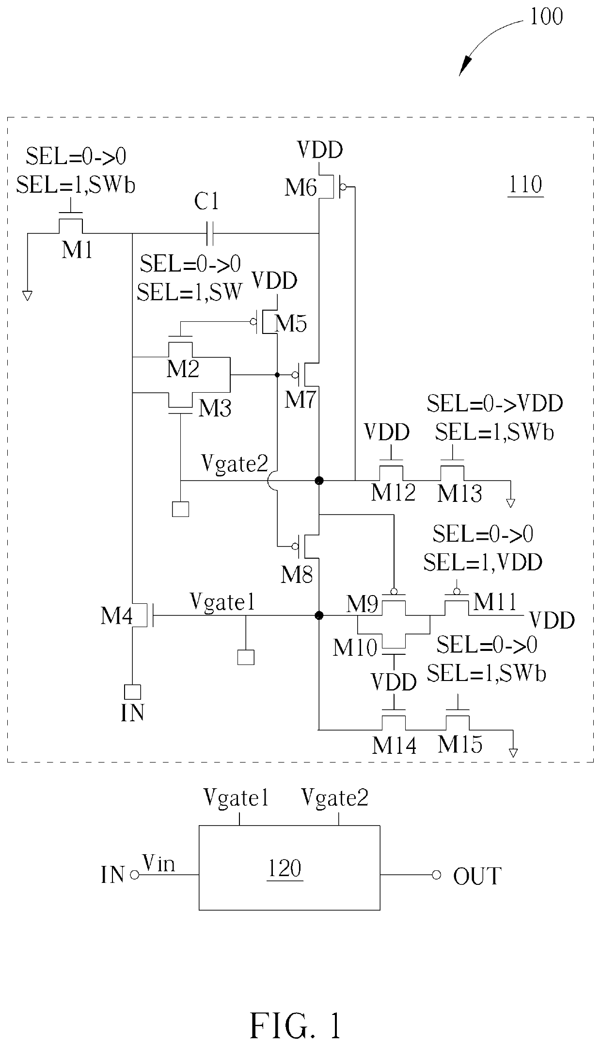
The present invention aims to provide an improved bootstrap switch device to overcome the aforementioned problem. The device can limit the voltage level of the input signal and turn off if it exceeds the power voltage, thereby disabling the signal path between the input and output terminals. This helps to address reliability issues caused by excessive voltage difference between the drain / source / gate of the NMOS and avoids leakage current problems.

Problems solved by technology

In some situations, when the transmission gate encounters the situation where the voltage level of the input signal is larger than the power voltage level, the P-type metal-oxide-semiconductor field effect transistors (PMOS) in the transmission gate will be passively conducted, making the transmission gate unable to effectively disable the signal transmission path in order to turning off the switch.
On the other hand, the Parasitic PN junction in the PMOS of the transmission gate may also generate leakage current, which has negative influence on the function of blocking signals.
However, when the voltage level of the input signal is larger than the power voltage level, a portion of bootstrap switches may cause the voltage difference between the drain / source / gate of the NMOS to be higher than the power voltage, which raises some reliability issues.

Method used


Image

  • Switch device with input limiting function
  • Switch device with input limiting function
  • Switch device with input limiting function

Examples


Embodiment Construction

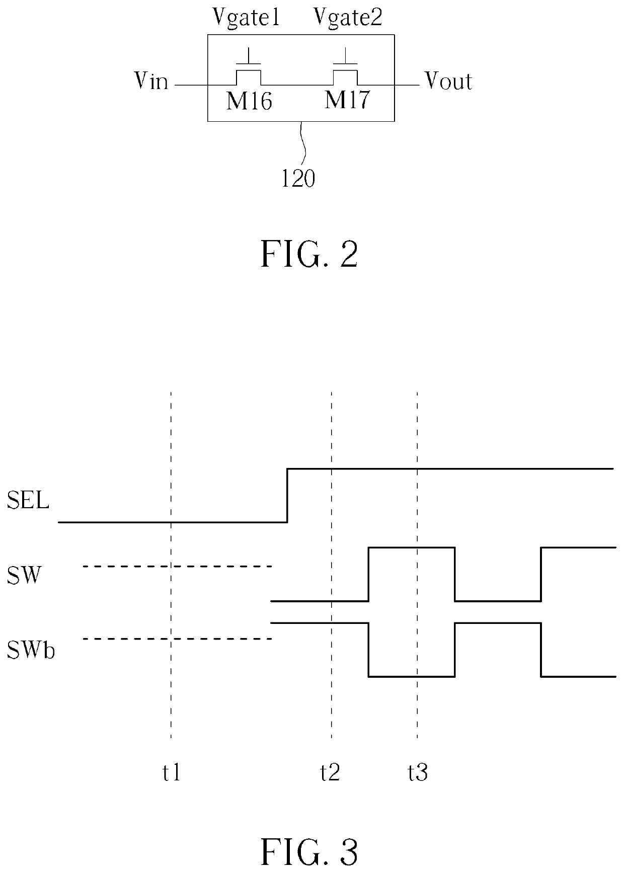
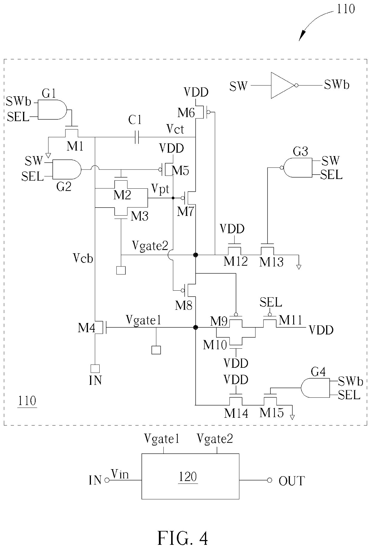
[0012]To solve the problem existing in related arts, the present invention proposes a switch device improved based on a bootstrap switch. Refer to FIG. 1, where the switch device 100 is composed of a switch controller 110 and a switch circuit 120. In an embodiment, the switch circuit 120 may comprise the transistors M16 and M17. As shown in FIG. 2, the gates of the transistor M16 and M17 are respectively controlled by the switch control signals Vgate1 and Vgate2 generated by the switch controller 110, and under the control of the switch control signals Vgate1 and Vgate2, the gates of the transistor M16 and M17 are also arranged to selectively deliver the input signal Vin at the input terminal as the output terminal Vout, and thereby achieve the functions of a switch.

[0013]The switch device 100 of the present invention comprises the following two main operation states: (1) When the input signal Vin is larger than the power voltage VDD, the switch circuit 120 is turned off to disable ...


PUM


Abstract

A switch device including a switch circuit and switch controller. The switch circuit comprises first and second switches to selectively enable a path between an input terminal and an output terminal. The switch controller refers to a selection signal and a switch signal to respectively generate a first switch control signal at a first switch control signal output terminal and a second switch control signal at a second switch control signal output terminal. When the voltage level of an input signal at the input terminal is larger than a power voltage, the switch controller generates the first switch control signal and the second switch control signal capable of turning off the switch circuit. When the voltage level of the input signal is not larger than the power voltage, the switch controller generates the first switch control signal and the second switch control signal according to the switch signal.

Description

BACKGROUND OF THE INVENTION1. Field of the Invention[0001]The present invention relates to a switch device, and more particularly, to a switch device with an input limiting function.2. Description of the Prior Art[0002]In related arts, the transmission gate is often used for transmitting control signals in an integrated circuit (IC). In some situations, when the transmission gate encounters the situation where the voltage level of the input signal is larger than the power voltage level, the P-type metal-oxide-semiconductor field effect transistors (PMOS) in the transmission gate will be passively conducted, making the transmission gate unable to effectively disable the signal transmission path in order to turning off the switch. On the other hand, the Parasitic PN junction in the PMOS of the transmission gate may also generate leakage current, which has negative influence on the function of blocking signals. To address this issue, a related art technique has proposed a bootstrap swi...

Claims


Application Information

Patent Timeline
Patent Type & Authority Patents(United States)
IPC IPC(8): H03K17/687H03K19/20H03M1/12
CPCH03K17/6872H03K19/20H03M1/12H03K17/08104H03K17/687H03K17/693H03K2217/0054H03K2017/066H03M1/122
Inventor XU, FENGWU, SHU DONGZHANG, ZHEN LIANG
Owner FARADAY TECH CORP
Learn More