Method for joining lead frames in a package assembly, method for forming a chip stack package, and a chip stack package

a technology of package assembly and lead frame, applied in the direction of electrical equipment, semiconductor devices, semiconductor/solid-state device details, etc., can solve the problems of reducing productivity, increasing processing time, and affecting the quality of finished products

Inactive Publication Date: 2004-01-22
SAMSUNG ELECTRONICS CO LTD
View PDF8 Cites 88 Cited by
  • Summary
  • Abstract
  • Description
  • Claims
  • Application Information

AI Technical Summary

Problems solved by technology

Such a drawback can result from oxidation of the plating layers 28 and 48.
The solder dipping process is performed after the package assembly p...

Method used


Image

  • Method for joining lead frames in a package assembly, method for forming a chip stack package, and a chip stack package
  • Method for joining lead frames in a package assembly, method for forming a chip stack package, and a chip stack package
  • Method for joining lead frames in a package assembly, method for forming a chip stack package, and a chip stack package

Examples


Embodiment Construction

[0029] Exemplary embodiments of the present invention will be described more fully below with reference to the accompanying drawings, in which exemplary embodiments of the invention are shown. The invention may, however, be embodied in many different forms and should not be construed as being limited to the embodiments set forth herein. Rather, these embodiments are provided so that this disclosure will be thorough and complete and will fully convey the concept of the present invention to those skilled in the art. In the drawings, the thickness of layers and regions are exaggerated for clarity. It should also be understood that when a layer is referred to as being "on" another layer or a substrate, it can be located directly on the other layer or the substrate, or intervening layers may be present. Throughout the specification, like numbers refer to like elements.

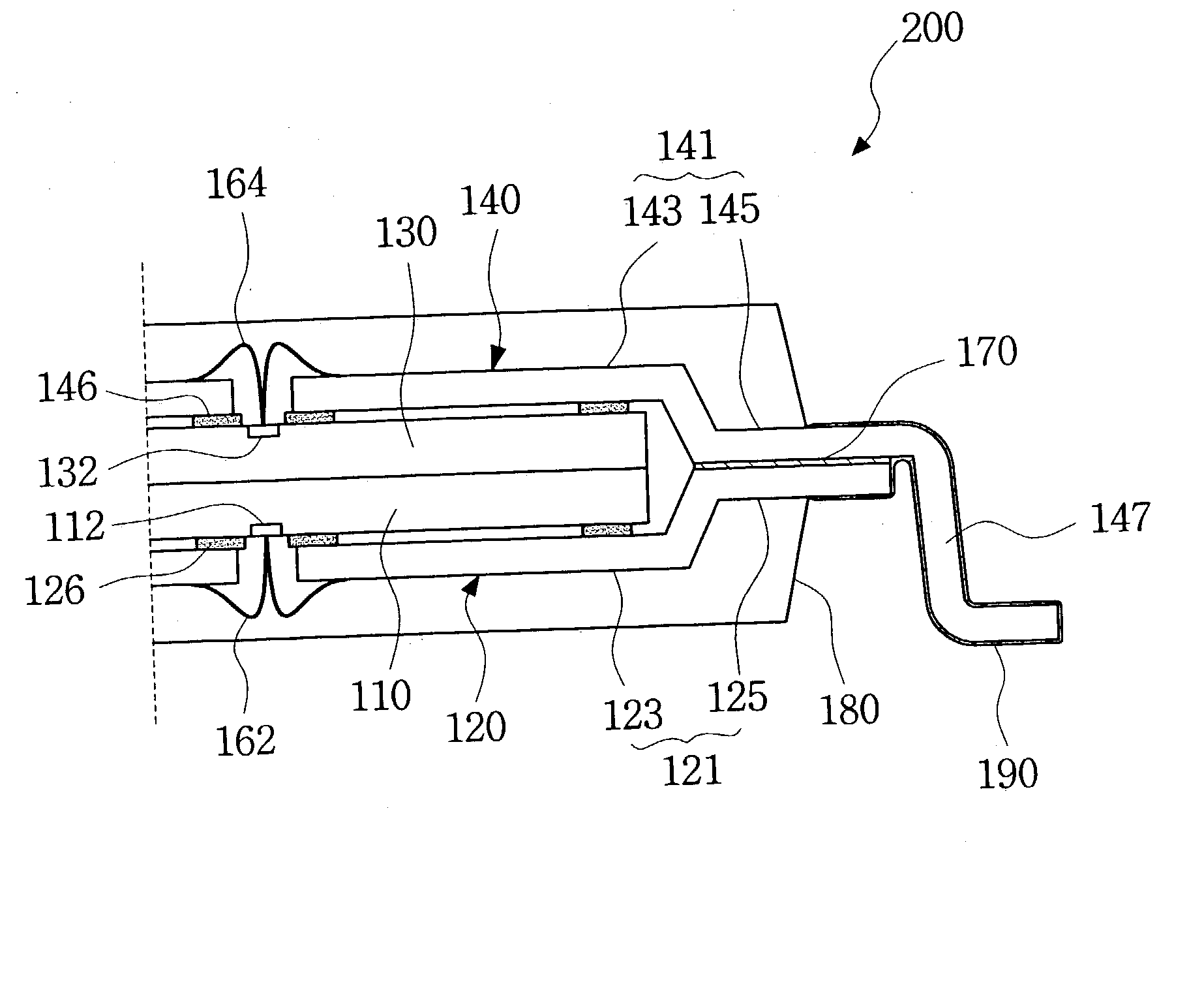
[0030] Referring to FIG. 3, a dual-die package 200 is shown as an example of a chip stack package formed by exemplary emb...


PUM


Abstract

A method for joining lead frames in a chip stack package or a package stack, a chip stack package, and a method of forming a chip stack package. A joining mediator is formed on joining portions of at least one lead frame. The joining mediator has an anti-oxidation property and an inter-metallic diffusion property, and may be formed of gold wires, gold bumps, gold bars, solder bumps, solder, or solder bars. By clamping or compressing the lead frames under heat and pressure, the joining mediator forms an inter-metallic joint layer that reliably interconnects the lead frames at the joining portions.

Description

[0001] This U.S. non-provisional application claims priority under 35 U.S.C. .sctn.119 to Korean Patent Application No. 2002-42539 filed Jul. 19, 2002, the contents of which are incorporated by reference in its entirety.[0002] 1. Field of the Invention[0003] The present invention relates generally to package assembly technology, and more particularly to a method for joining two or more lead frames in a chip stack package or a package stack, a method for forming a chip stack package, and a chip stack package.[0004] 2. Description of the Related Art[0005] Developments in semiconductor technology and high demands from consumers have created a trend in the electronics industry towards higher memory capacity and smaller footprints. To meet these demands, stack techniques such as stacking semiconductor chips or stacking packages have been introduced.[0006] The package stack has the advantage of reliability since each assembled package has passed both functional and reliability tests. Furt...

Claims


Application Information

Patent Timeline
IPC IPC(8): H01L25/18H01L23/28H01L23/495H01L23/50H01L25/065H01L25/07
CPCH01L23/4951H01L23/49537H01L2224/45144H01L2924/01033H01L2924/01006H01L24/48H01L24/32H01L2924/01082H01L23/49558H01L23/49575H01L2224/32014H01L2224/32245H01L2224/48091H01L2224/48247H01L2224/4826H01L2224/73215H01L2924/01004H01L2924/01005H01L2924/01047H01L2924/0105H01L2924/01078H01L2924/01079H01L2924/00014H01L2924/00H01L24/45H01L2224/45015H01L2924/181H01L2924/20753H01L2224/05599H01L23/28
Inventor KIM, PYOUNG WANLEE, SANG HYEOPLEE, CHANG CHEOLLEE, GUN AH
Owner SAMSUNG ELECTRONICS CO LTD
Why Eureka
Try Eureka