Copper recess process with application to selective capping and electroless plating
What is AI technical title?
AI technical title is built by Patsnap AI team. It summarizes the technical point description of the patent document.
a copper recess and electroless plating technology, applied in the direction of semiconductor devices, semiconductor/solid-state device details, electrical apparatus, etc., can solve the problems of affecting the effective dielectric constant of the overall dielectric material, and substantially distorting the dielectric constan
Active Publication Date: 2004-06-17
TAIWAN SEMICON MFG CO LTD
View PDF1 Cites 131 Cited by
Summary
Abstract
Description
Claims
Application Information
AI Technical Summary
This helps you quickly interpret patents by identifying the three key elements:
Problems solved by technology
Method used
Benefits of technology
Problems solved by technology
One drawback of using low-K dielectrics in the BEOL interconnection layers is that the low-K dielectrics are more sensitive to metal migration (e.g., copper migration) than were the higher-K dielectrics.
However, this dielectric cap usually has higher dielectric constant and will greatly affect the effective dielectric constant of the overall dielectric material between metal features.
However, if the dielectric cap is formed above a certain thickness, it will substantially distort the dielectric constant of the interconnect layer above a desired level.
Method used
Image
Click on the blue label to locate the original text in one second.
Reading with bidirectional positioning of images and text.
Examples
Embodiment Construction
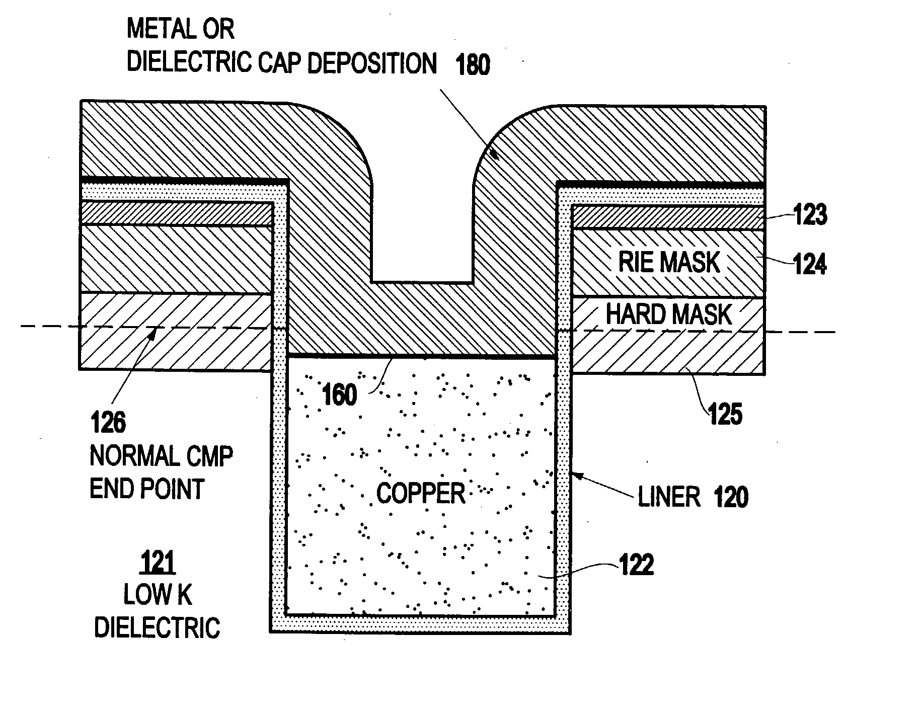
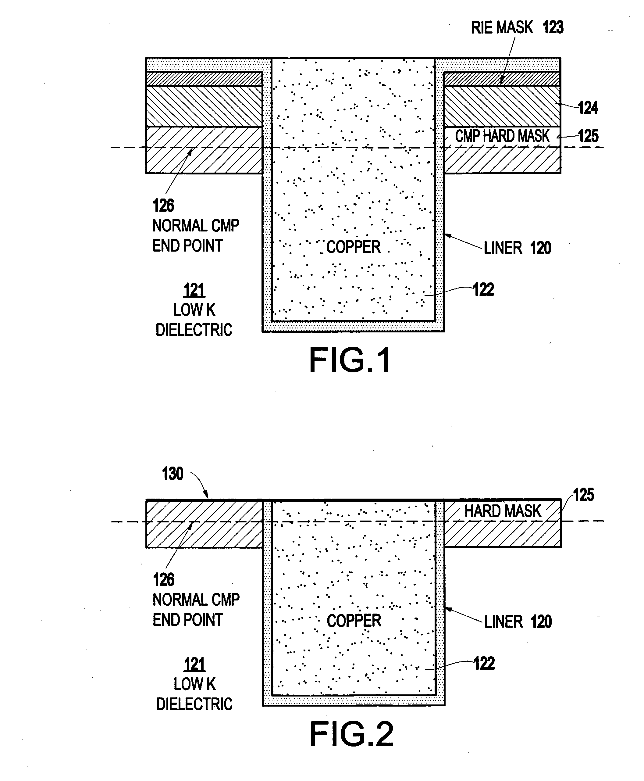
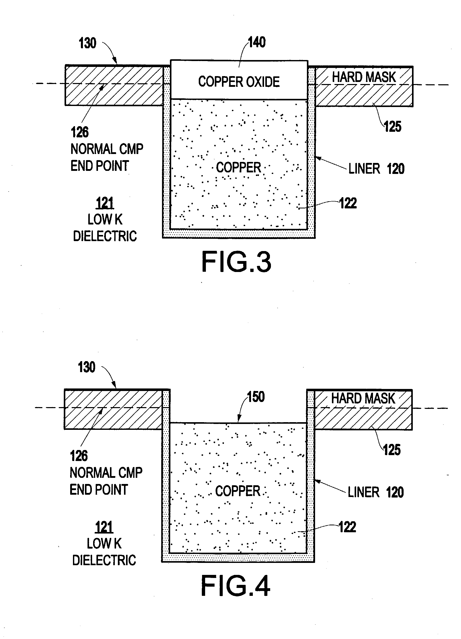
[0024] As mentioned above, the conventional use of a high-K dielectric cap presents a number of disadvantages. The invention overcomes such disadvantages by forming the cap material only above metal areas such as wiring and interlevel interconnections. More specifically, as shown below, the invention polishes the interconnection layer down to a predetermined level, forms recesses in the tops of the metal portions, deposits the cap material over the entire interconnection layer, and then polishes the interconnection layer so that the cap material only remains within the recesses above the metal portions. Performing such processing, the invention substantially reduces the amount of high-K dielectric cap material within the structure, thereby avoiding the problems that are encountered when a blanket layer of dielectric cap material is utilized (discussed above).
[0025] The processing used to achieve the inventive structure is shown in FIGS. 1-12, which represent multiple embodiments of ...
PUM
Abstract
An integrated circuit structure is disclosed that has a layer of logical and functional devices and an interconnection layer above the layer of logical and functional devices. The interconnection layer has a substrate, conductive features within the substrate and caps positioned only above the conductive features.
Description
[0001] 1. Field of the Invention[0002] The present invention generally relates to insulators / conductors above copper wiring connections on exterior interconnectionlayers of an integrated circuit structure, and more particularly to an improved process and structure for forming such interconnection layers.[0003] 2. Description of the Related Art[0004] Integrated circuitprocessing can be generally divided into front end of line (FEOL) and back and of line (BEOL) processes. During FEOL processing, the various logical and functional devices are manufactured. The FEOL processing will generally form many layers of logical and functional devices. Layers of interconnections are formed above these logical and functional layers during the BEOL processing to complete the integrated circuit structure. Therefore, BEOL processing generally involves the formation of insulators and conductive wiring and contacts.[0005] Recently, insulators (dielectrics) that have a lower dielectric constant (and a...
Claims
Application Information
Patent Timeline
Application Date:The date an application was filed.
Publication Date:The date a patent or application was officially published.
First Publication Date:The earliest publication date of a patent with the same application number.
Issue Date:Publication date of the patent grant document.
PCT Entry Date:The Entry date of PCT National Phase.
Estimated Expiry Date:The statutory expiry date of a patent right according to the Patent Law, and it is the longest term of protection that the patent right can achieve without the termination of the patent right due to other reasons(Term extension factor has been taken into account ).
Invalid Date:Actual expiry date is based on effective date or publication date of legal transaction data of invalid patent.

