Data erasing method, and memory apparatus having data erasing circuit using such method

a data eraser and memory device technology, applied in semiconductor devices, transistors, instruments, etc., can solve the problems of increasing power consumption, taking a long time to increasing etc., to reduce the time required to erase data, boost the potential of semiconductor substrates, and reduce the effect of time required

Inactive Publication Date: 2005-01-20
SONY CORP
View PDF2 Cites 28 Cited by
  • Summary
  • Abstract
  • Description
  • Claims
  • Application Information

AI Technical Summary

Benefits of technology

The present invention relates to a data erasing method and a memory apparatus that use an erasing voltage to discharge electric charges accumulated in a floating gate. The invention aims to reduce the time required to boost the potential of the semiconductor substrate and prevent the leakage of electric charges during the boost. By applying the erasing voltage between the semiconductor substrate and the control gate while boosting the potential of the semiconductor substrate side and making the potential of the control gate to a predetermined potential, the invention achieves these technical effects.

Problems solved by technology

The technical problem addressed in this patent text is the inefficient and time-consuming data erasing process in conventional memory devices due to the leakage of electric charges and the resulting capacity coupling between the control gate and semiconductor substrate. This leads to increased power consumption and a need for improved methods for data erasure.

Method used


Image

  • Data erasing method, and memory apparatus having data erasing circuit using such method
  • Data erasing method, and memory apparatus having data erasing circuit using such method
  • Data erasing method, and memory apparatus having data erasing circuit using such method

Examples


Embodiment Construction

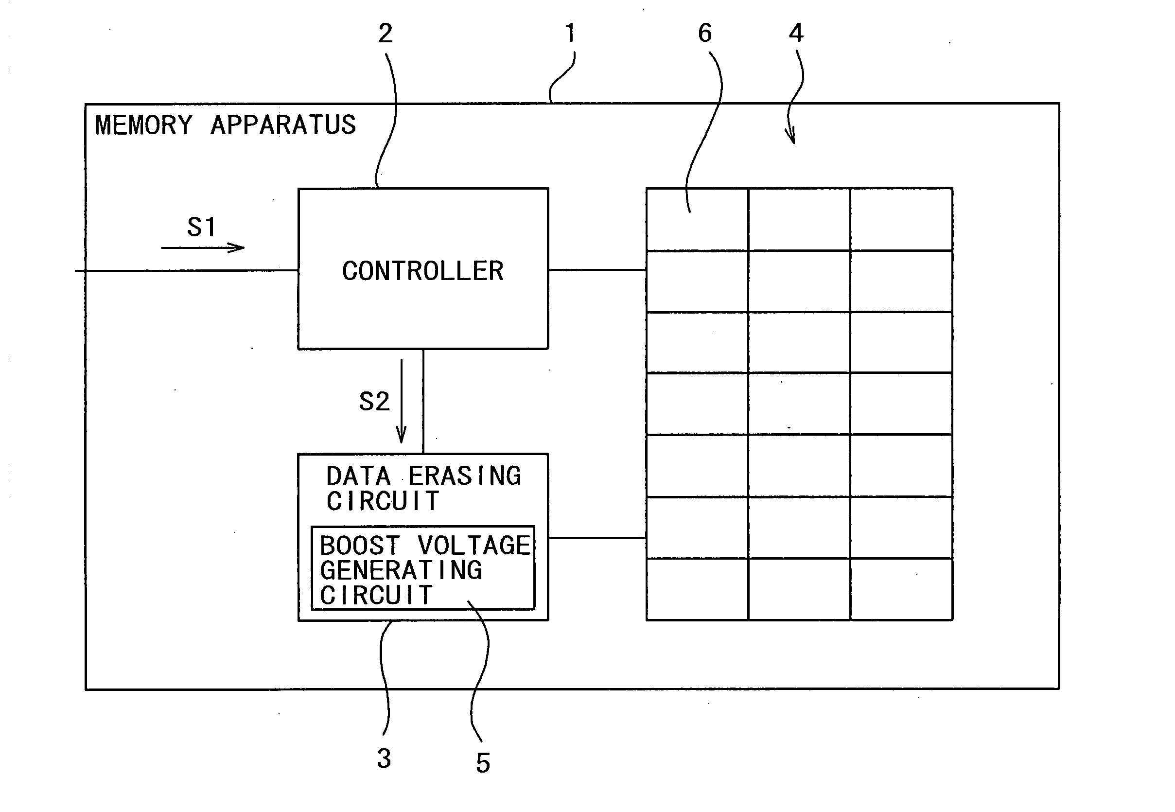
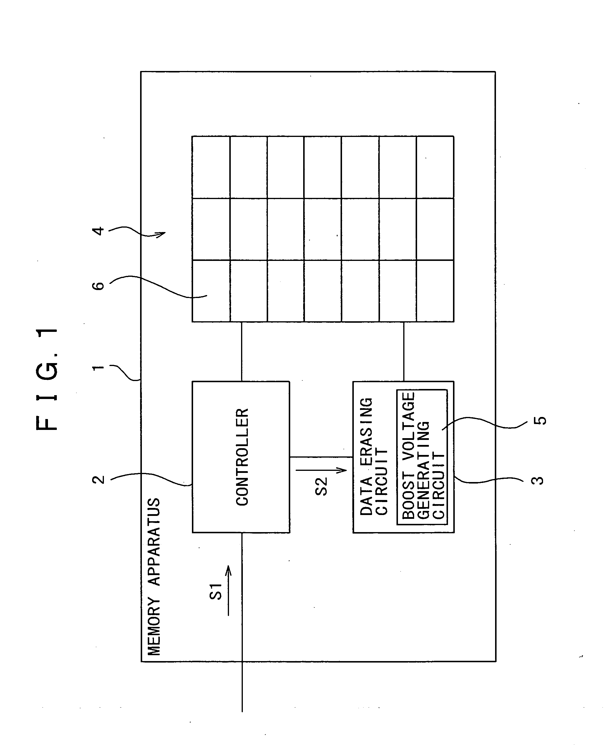
[0029] A memory apparatus according to the present invention comprises a storage area composed of a controller, a plurality of storage elements, and a boost voltage generating circuit.

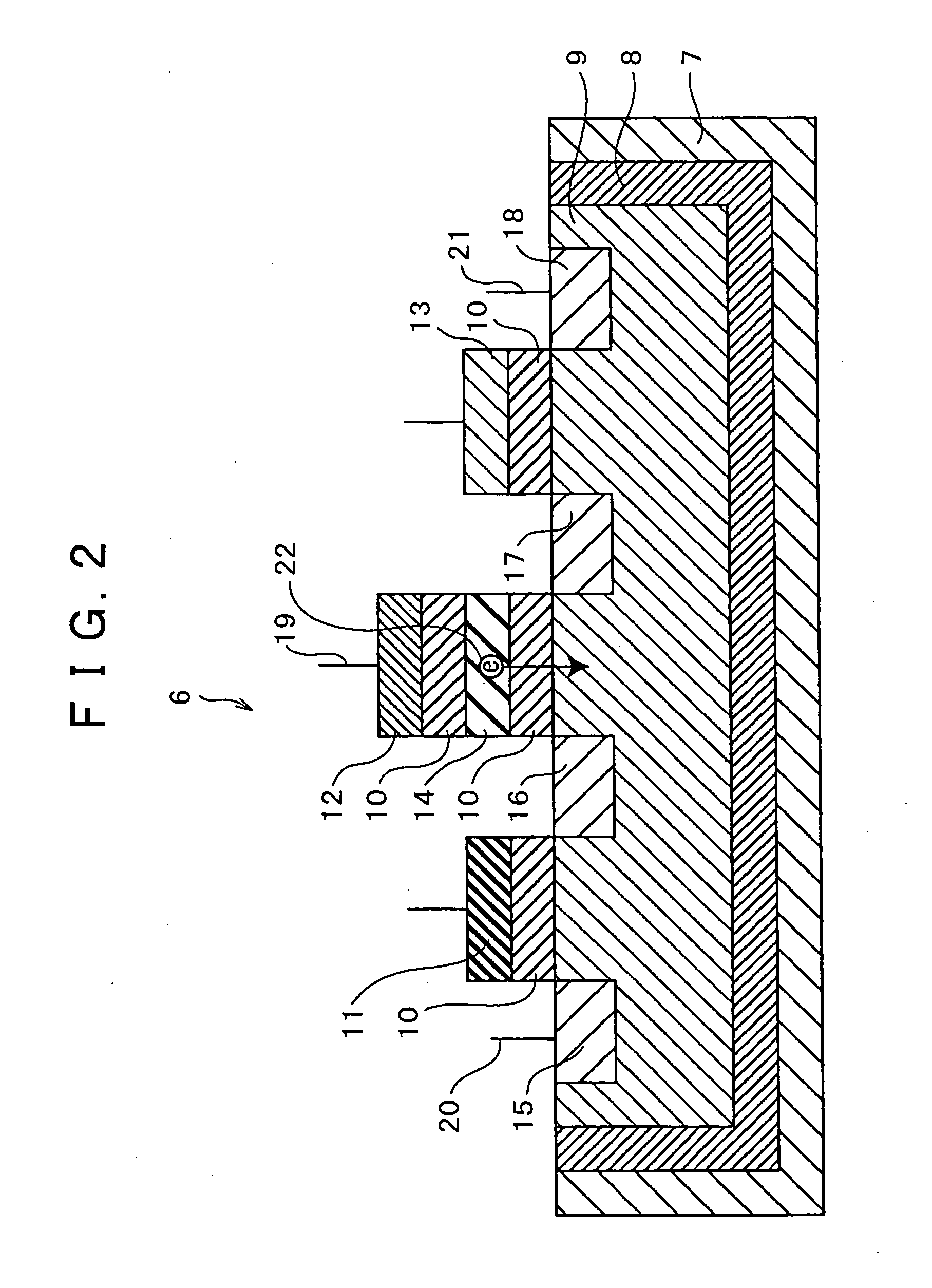
[0030] This storage element has a control gate disposed above a semiconductor substrate, and a floating gate for accumulating electric charges between the semiconductor substrate and the control gate, and is constructed such that data storage can be effected based on presence or absence of electric charges accumulated in the floating gate.

[0031] Further, the storage element is constructed such that a switch is connected to the control gate, and this switch has a predetermined time constant when changing from a disconnected state to a connected state.

[0032] In the case where data erasing operation is effected in the memory apparatus of the foregoing structure, the electric charges accumulated in the floating gate are discharged to erase the stored data by applying an erasing voltage between the semic...


PUM


Abstract

The present invention is to propose an data erasing method, a memory apparatus, and a data erasing circuit which are able to reduce the time required to boost the potential of the semiconductor substrate thereby to reduce the time required to erase data. Namely, a memory apparatus having a data erasing circuit that erases stored data by applying an erasing voltage between a semiconductor substrate and a control gate so as to discharge electric charges accumulated in a floating gate is disclosed. In this case, the data erasing circuit boosts a potential of the semiconductor substrate side while placing the control gate into its floating state; and applies an erasing voltage between the semiconductor substrate and the control gate to make the potential of the control gate to a predetermined potential.

Description


Claims


Application Information

Patent Timeline
Owner SONY CORP
Why Eureka
Try Eureka