Micro structure with interlock configuration

a micro-structure and configuration technology, applied in the field of micro-structures, can solve the problems of increasing the cost of the structure, the camber of the cantilever, and the difficulty of firmly fixing the polysilicon layer, and achieve the effect of suppressing the falling of the conductive member

Inactive Publication Date: 2005-02-10
YAMAHA CORP
View PDF5 Cites 53 Cited by
  • Summary
  • Abstract
  • Description
  • Claims
  • Application Information

AI Technical Summary

Benefits of technology

An object of this invention is to provide a micro structure and its manufacture method capable of preventing a conductive member such as an electrode and a wiring line from falling out of a via hole.
As above, the interlock structure of a via hole and an connection portion of the conductive member constitutes a strong mechanical interlock structure. It is possible to suppress the conductive member from falling out of the via hole.

Problems solved by technology

It is not easy, however, to firmly fix a polysilicon layer by only the bottom surface of the contact column.
It is difficult, however, to sufficiently suppress camber of the cantilever.
New facilities are required to be introduced, resulting in a cost rise.
With a dry etching method using as etching gas a mixture gas of Cl2 or HBr gas, and O2 gas, an etching rate is slow so that lower productivity cannot be avoided when thick silicon is etched.
It is difficult to have a good isotropic shape.

Method used


Image

  • Micro structure with interlock configuration
  • Micro structure with interlock configuration
  • Micro structure with interlock configuration

Examples


Embodiment Construction

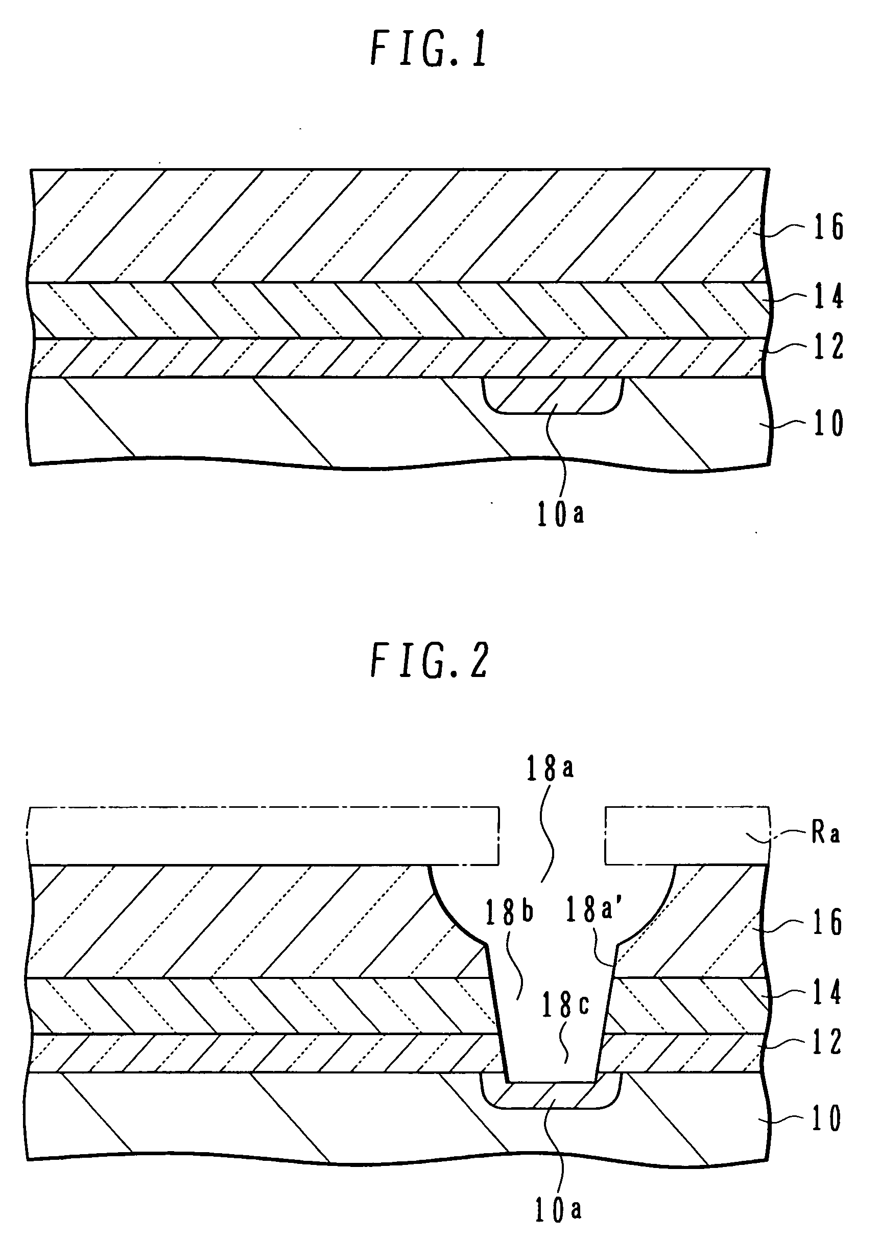
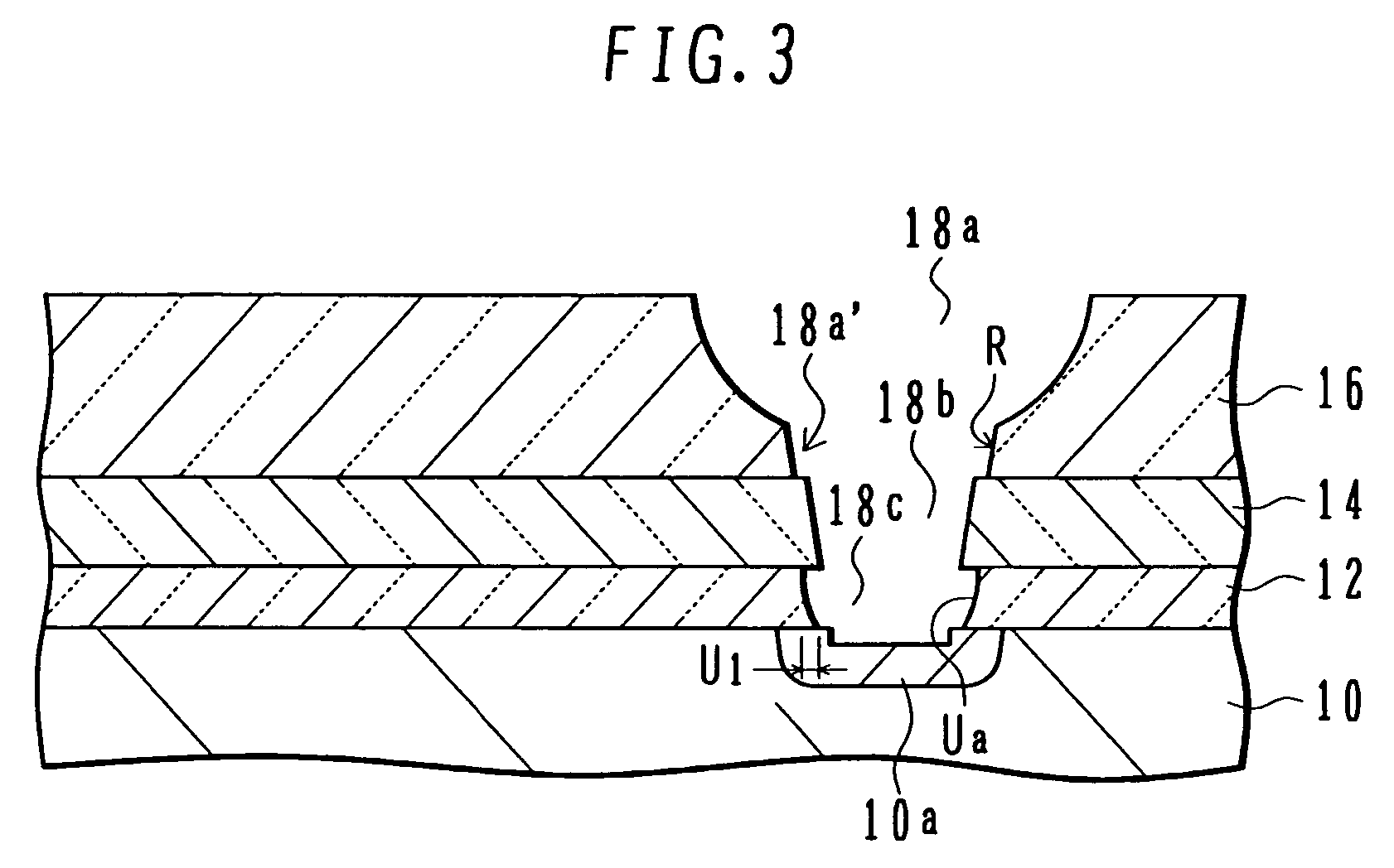
FIGS. 1 to 6 are cross sectional views illustrating main processes of a micro structure manufacture method according to an embodiment of the present invention. Processes (1) to (6) illustrated in FIGS. 1 to 6 will be described in this order.

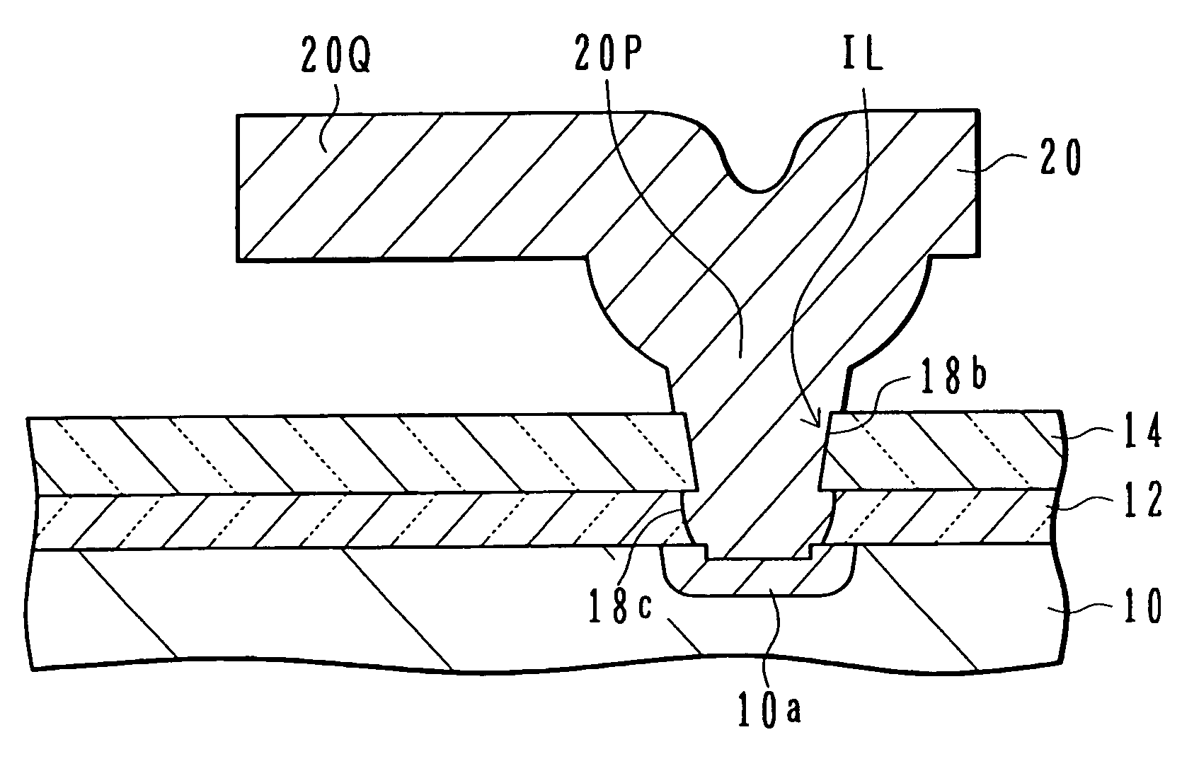
(1) On one principal surface of a semiconductor substrate 10 made of, for example, single crystal silicon, a connection region 10a is formed. On the principal surface, a first insulating film 12, a second insulating film 14 and a third insulating film 16 are stacked sequentially. For example, the connection region 10a is an n-type and is formed in a p-type region. The insulating film 12 is used as a pad film, and made of, for example, a silicon oxide film having a thickness of 150 to 300 nm, more preferably 200 to 250 nm. This silicon oxide film is formed by a thermal oxidation method although it may be formed by a chemical mechanical deposition (CVD) method or the like.

FIG. 42 schematically shows the structure of a CVD system. In a hermetic ch...


PUM


Abstract

A micro structure has: a semiconductor substrate; an insulating film having a via hole and formed on the semiconductor substrate; an interlock structure formed on a side wall of the via hole and having a retracted portion and a protruded portion above the retracted portion; a conductive member having at one end a connection portion formed burying the via hole and an extension portion continuous with the connection portion and extending along a direction parallel to a surface of the semiconductor substrate.

Description

CROSS REFERENCE TO RELATED APPLICATION This application is based on and claims priorities of Japanese Patent Applications No. 2003-205411 filed on Aug. 1, 2003, No. 2003-314546 and No. 2003-314547 both filed on Sep. 5, 2003, and No. 2004-159017 filed on May 28, 2004, the entire contents of which are incorporated herein by reference. BACKGROUND OF THE INVENTION A) Field of the Invention The present invention relates to a micro structure suitable for use in a micro-electro-mechanical system (MEMS). B) Description of the Related Art As a micro structure, an acceleration sensor is known having a parallel plate capacitor formed on a silicon substrate (e.g., refer to Japanese Patent Laid-open Publication No. 2001-121499 (U.S. Ser. No. 09 / 395,711 filed on Sep. 5, 2000) which is incorporated herein by reference). According to this prior art, a fixed electrode and a movable electrode constituting a parallel plate capacitor are both made of a polysilicon layer whose portion is fixed to ...

Claims


Application Information

Patent Timeline
Patent Type & Authority Applications(United States)
IPC IPC(8): B81B3/00H01L21/768
CPCB81B3/0054B81B2203/0118B81B3/001H01L21/76804H01L21/76877B81B2203/0307
Inventor SUZUKI, TAMITO
Owner YAMAHA CORP
Why Eureka
Try Eureka