Micro structure with interlock configuration
a micro-structure and configuration technology, applied in the field of micro-structures, can solve the problems of increasing the cost of the structure, the camber of the cantilever, and the difficulty of firmly fixing the polysilicon layer, and achieve the effect of suppressing the falling of the conductive member
- Summary
- Abstract
- Description
- Claims
- Application Information
AI Technical Summary
Benefits of technology
Problems solved by technology
Method used
Image
Examples
Embodiment Construction
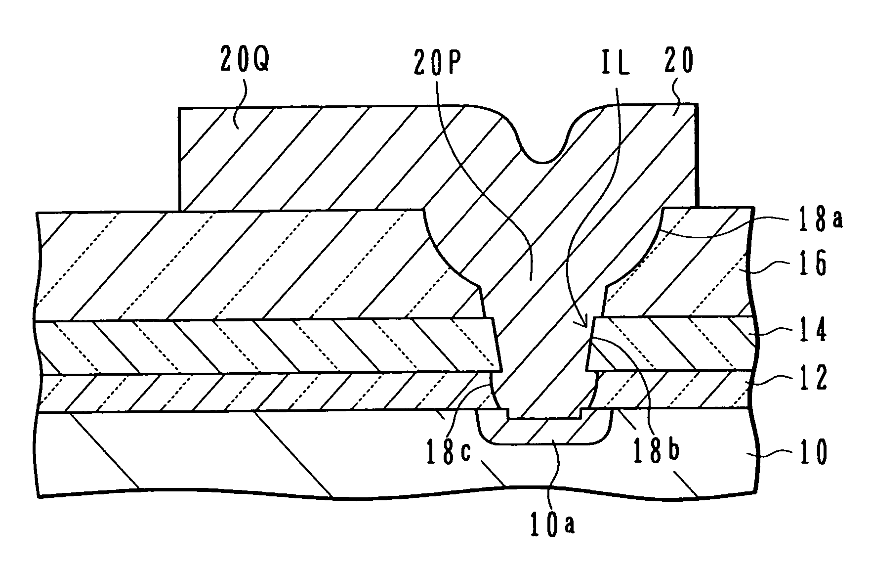
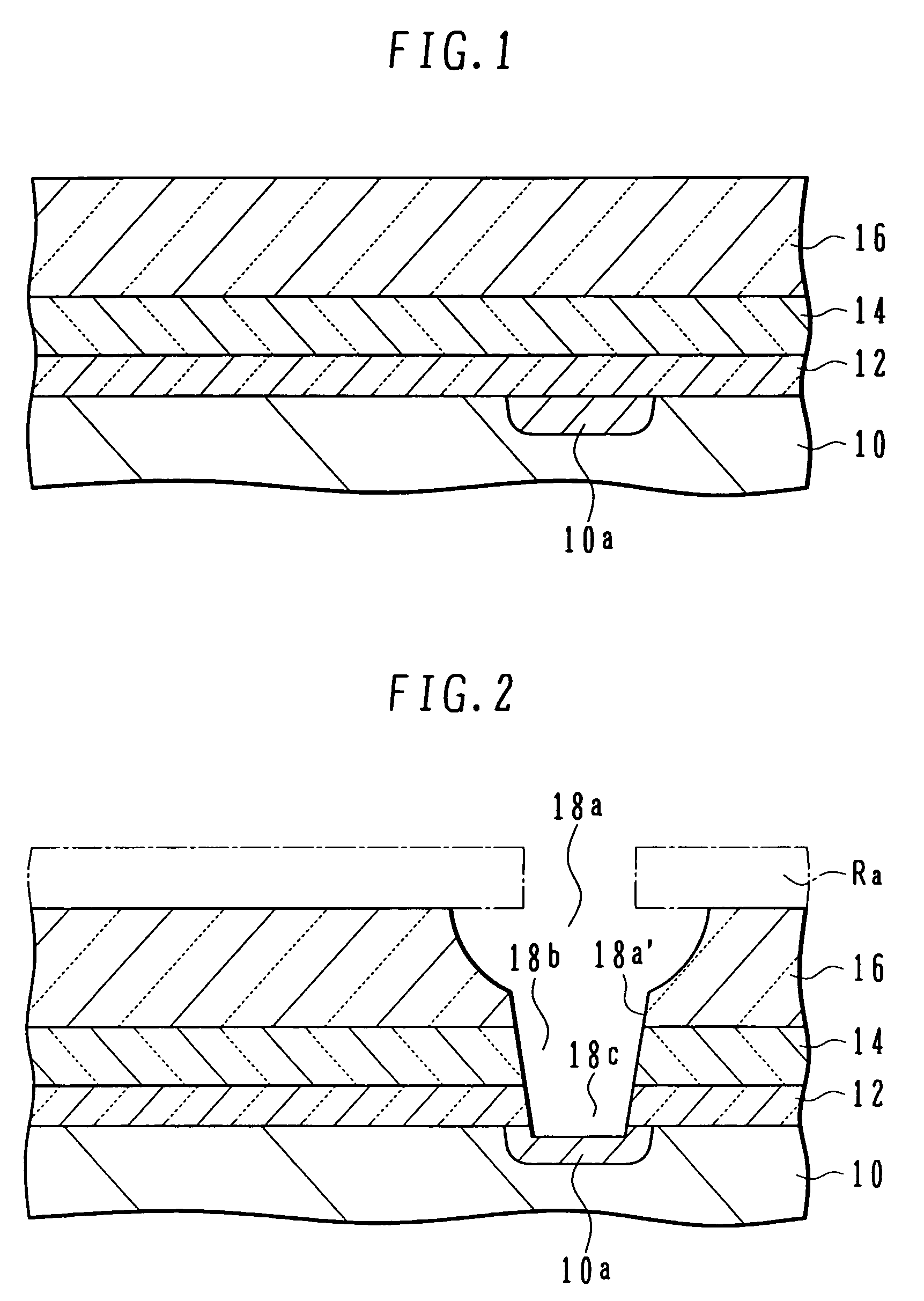
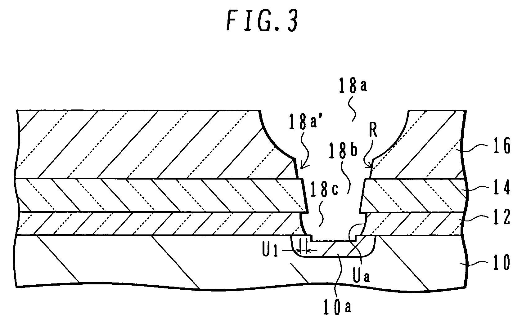
[0043]FIGS. 1 to 6 are cross sectional views illustrating main processes of a micro structure manufacture method according to an embodiment of the present invention. Processes (1) to (6) illustrated in FIGS. 1 to 6 will be described in this order.
[0044](1) On one principal surface of a semiconductor substrate 10 made of, for example, single crystal silicon, a connection region 10a is formed. On the principal surface, a first insulating film 12, a second insulating film 14 and a third insulating film 16 are stacked sequentially. For example, the connection region 10a is an n-type and is formed in a p-type region. The insulating film 12 is used as a pad film, and made of, for example, a silicon oxide film having a thickness of 150 to 300 nm, more preferably 200 to 250 nm. This silicon oxide film is formed by a thermal oxidation method although it may be formed by a chemical mechanical deposition (CVD) method or the like.
[0045]FIG. 42 schematically shows the structure of a CVD system. ...
PUM
 Abstract
Description
Claims
Application Information


