Nanotube device structure and methods of fabrication

a technology of nanotubes and devices, applied in nanoelectromechanical switches, relays, instruments, etc., can solve the problems of high power consumption, density and operation speed of mos digital circuits, and limited density of bipolar digital integrated circuits

Active Publication Date: 2005-02-17
NANTERO
View PDF42 Cites 142 Cited by
  • Summary
  • Abstract
  • Description
  • Claims
  • Application Information

AI Technical Summary

Benefits of technology

[0027] Under another aspect of the invention, the upper surface of the nanotube switching element includes an area defining the control electrode and wherein the area includes at least one dimension that is sub-lithographic.
[0028] Under another aspect of the invention, the one...

Problems solved by technology

However, the density of bipolar digital integrated circuits is limited by their high power consumption and the ability of packaging technology to dissipate the heat produced while the circuits are operating.
The density and operating speed of MOS digital circuits are still limited by the need to dissipate the heat produced when the device is operating.
Digital logic integrated circuits constructed from bipolar or MOS devices do not function correctly under conditions of high heat or extreme environment.
As leakage current increases, the operating temperature of the device rises, the power consumed by the circuit increases, and the difficulty of discriminating the off state from the on state reduces circuit reliability.
Conventional digital logic circuits also short intern...

Method used


Image

  • Nanotube device structure and methods of fabrication
  • Nanotube device structure and methods of fabrication
  • Nanotube device structure and methods of fabrication

Examples


Embodiment Construction

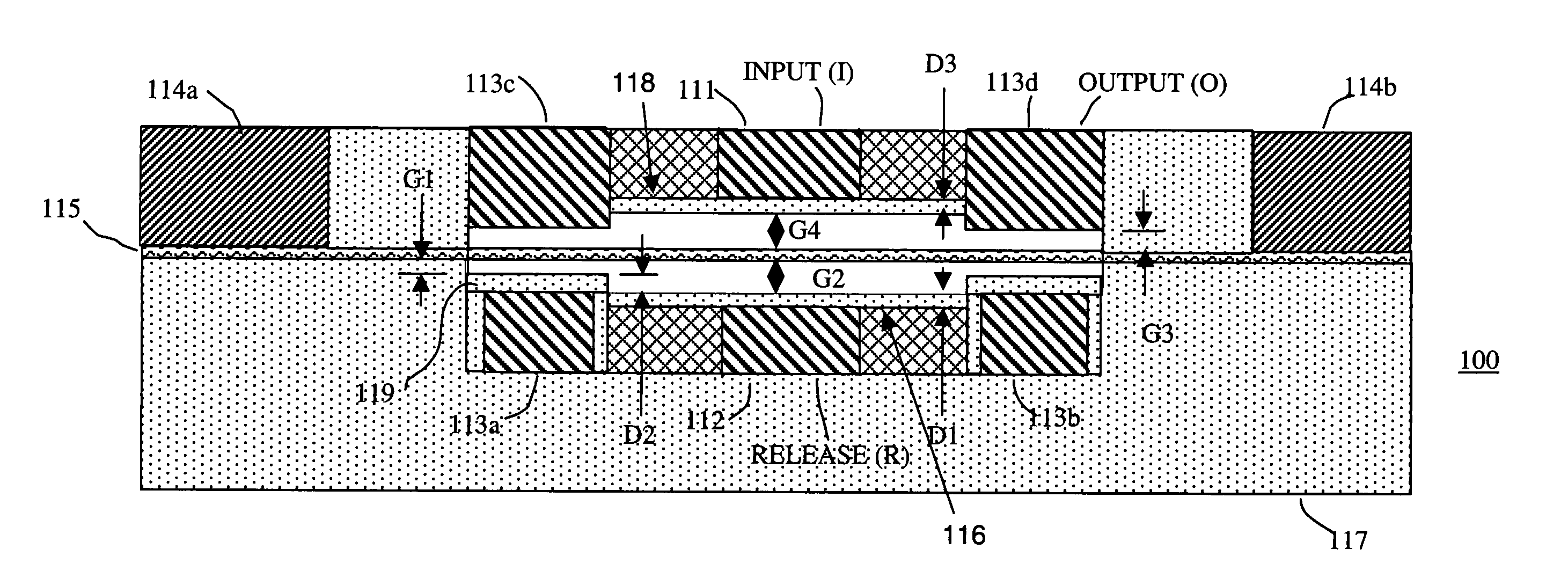
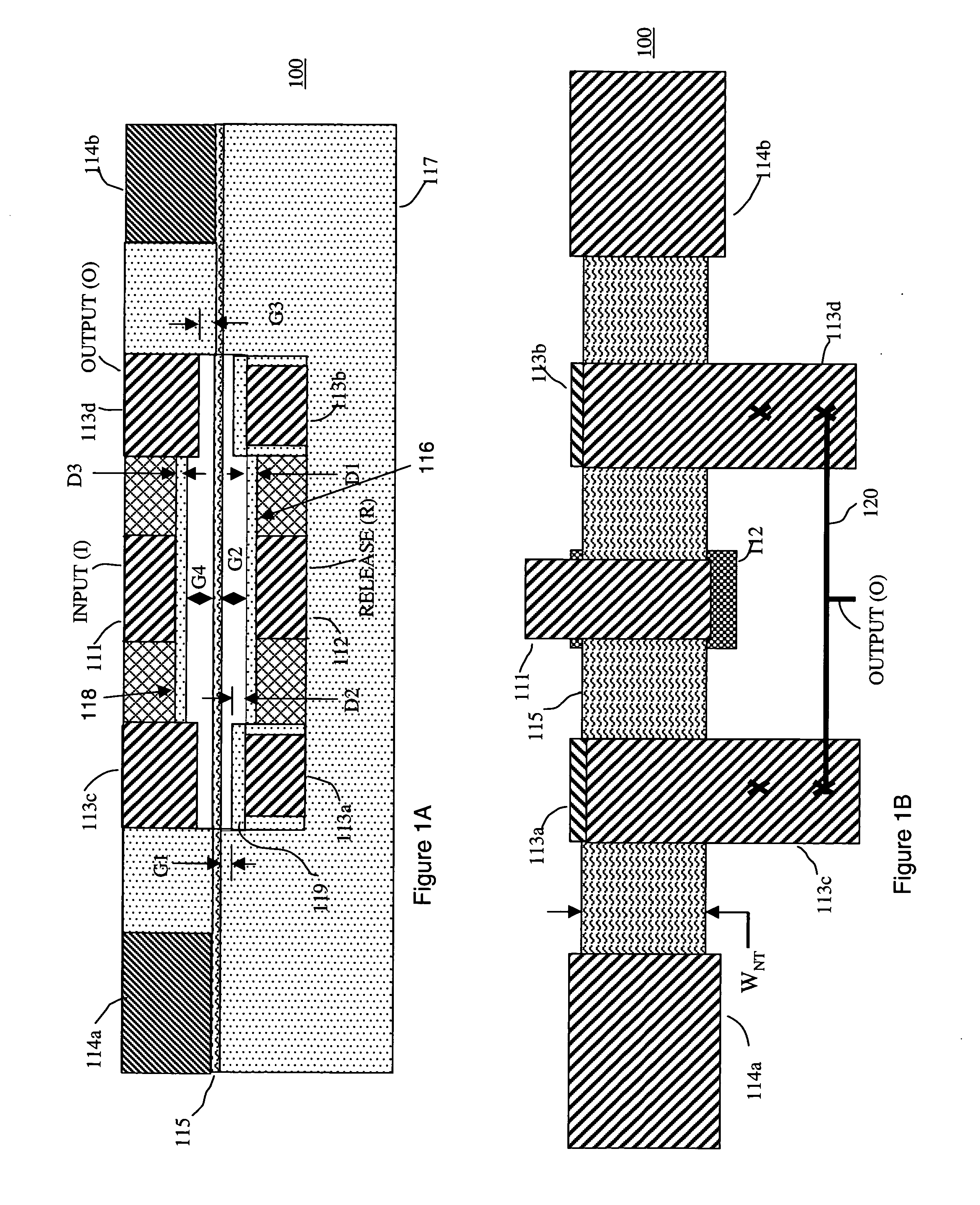
[0035] Preferred embodiments of the invention provide switching elements in which a nanotube-based channel may be controllably formed, under the influence of a control node, so that a signal may be transferred to an output node. The transferred signal may be a varying signal or a reference signal, depending on the manner in which the switching element is utilized and arranged. Preferred embodiments non-volatilely maintain the state of the nanotube switching element. Improved methods of manufacturing such devices are also provided.

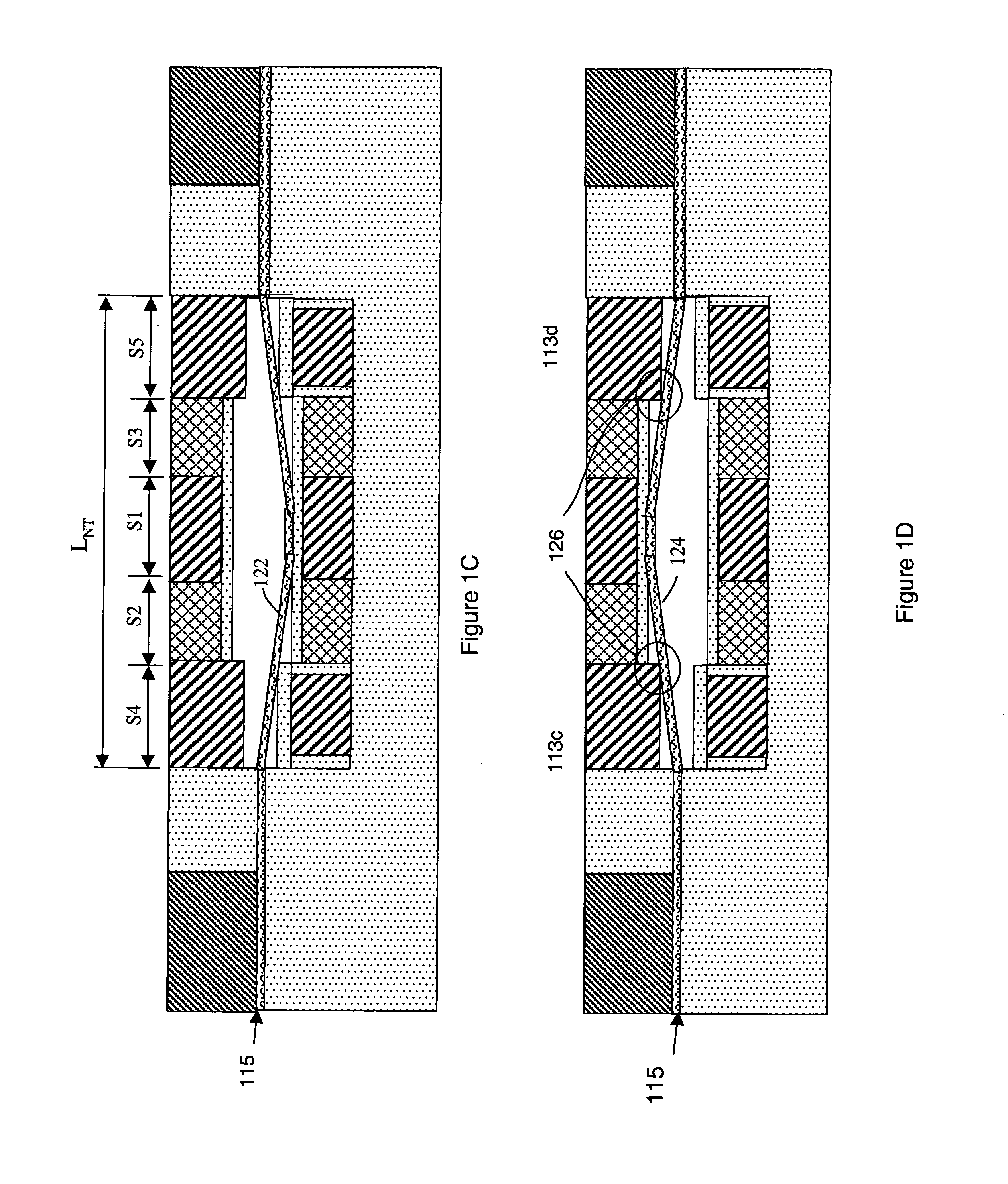
[0036]FIG. 1A is a cross sectional view of a preferred nanotube switching element 100. Nanotube switching element includes a lower portion having an insulating layer 117, release electrode 112, output electrodes 113a,b. Nanotube switching element further includes an upper portion having input electrode 111, output electrodes 113c,d, and signal electrodes 114a,b. A nanotube channel element 115 is positioned between and held by the upper and lower portions. ...


PUM

PropertyMeasurementUnit
Structureaaaaaaaaaa
Electrical conductoraaaaaaaaaa
Areaaaaaaaaaaa

Abstract

Nanotube device structures and methods of fabrication. Under one embodiment, a method of forming a nanotube switching element includes forming a first structure having at least one output electrode, forming a conductive article having at least one nanotube, and forming a second structure having at least one output electrode and positioning said second structure in relation to the first structure and the conductive article such that the output electrode of the first structure is opposite the output electrode of the second structure and such that a portion of the conductive article is positioned therebetween. At least one signal electrode is provided in electrical communication with the conductive article having at least one nanotube, and at least one control electrode is provided in relation to the conductive article such that the conductive electrode may control the conductive article to form a channel between the sginal electrode and at least one of the output electrodes. The first and second structures each include a respective second output electrode and wherein the second electrodes are positioned opposite each other with the conductive article positioned therebetween. The control electrode and the second control electrode includes an insulator layer on a surface facing the conductive article.

Description

CROSS-REFERENCE TO RELATED APPLICATIONS [0001] This application claims priority under 35 U.S.C. § 119(e) to U.S. Provisional Pat. Apl., Ser. No. 60 / 494,889, filed on Aug. 13, 2003, entitled Nanoelectromechanical Nanotube-Based Logic, which is incorporated herein by reference in its entirety. This application also claims priority under 35 U.S.C. § 119(e) to U.S. Provisional Pat. Apl., Ser. No. 60 / 580,879, filed on Jun. 18, 2004, entitled Carbon Nanotube (NCT) Device Structure and Methods of Fabrication, which is incorporated herein by reference in its entirety. [0002] This application is related to the following references: [0003] U.S. patent application Ser. No. ______ not yet assigned, filed on date even herewith, entitled Nanotube-Based Switching Elements; [Nan-31][0004] U.S. patent application Ser. No. ______ not yet assigned, filed on date even herewith, entitled Nanotube-Based Switching Elements And Logic Circuits; [Nan-78][0005] U.S. patent application Ser. No. ______ not yet ...

Claims


Application Information

Patent Timeline
IPC IPC(8): G11C13/02H01H1/027H01H59/00H01L21/00H01L27/28H01L29/06H01L29/73H01L29/78H01L51/30
CPCB82Y10/00Y10T29/49105G11C23/00H01H1/0094H01H1/027H01H2001/0005H01L27/28H01L29/0665H01L29/0673H01L29/73H01L29/78H01L51/0048H01L51/0508Y10S977/755Y10S977/733Y10S977/938Y10S977/725G11C13/025H10K19/00H10K85/221H10K10/46
Inventor BERTIN, CLAUDE L.RUECKES, THOMASSEGAL, BRENT M.
Owner NANTERO
Why Eureka
Try Eureka