Imaging device

a technology of image quality and image, applied in the field of image quality, can solve the problems of large aliasing noise, inability to produce excellent image quality, and difficulty in detecting pixels and zooming operations, and achieve the effect of excellent image quality

Active Publication Date: 2005-03-31
PANASONIC SEMICON SOLUTIONS CO LTD
View PDF10 Cites 20 Cited by
  • Summary
  • Abstract
  • Description
  • Claims
  • Application Information

AI Technical Summary

Benefits of technology

[0010] In view of the above problem, an object of the present invention is to provide an imaging device which produces an image with a resolution lower than an original resolution of a solid-state imaging element and excellent image quality.
[0012] According to this construction, the electric charges stored in the photoelectric conversion elements of the same color in each portion of L rows and C columns are added together, to obtain the resulting electric charge. This produces an effect of a spatial low pass filter, and therefore reduces signal components exceeding a Nyquist frequency corresponding to the target resolution. As a result, aliasing noise in the image with the target resolution is reduced, and therefore image quality is improved, when compared with a conventional resolution reduction technique of discarding pixels, which does not produce the effect of the spatial low pass filter.
[0015] Which is to say, the image with the target resolution obtained by the imaging device has a higher level of high-frequency components in the vicinity of the Nyquist frequency corresponding to the target resolution.
[0017] According to this construction, the level of high-frequency signal components is further improved. As a consequence, excellent image quality can be achieved.
[0019] According to this construction, pixels with different colors are not located close to each other, as a result of the charge addition. Respective pixels with all of the colors are more likely to be evenly arranged. As a consequence, excellent image quality can be achieved.
[0021] According to this construction, a pixel with a particular color lies precisely midst between two pixels with a different color, as a result of the charge addition. Thus, respective pixels with all of the colors are arranged at even intervals. As a consequence, excellent image quality can be achieved.

Problems solved by technology

However, such a conventional technique of discarding pixels and performing a zoom operation can not produce an image with excellent image quality in addition to a resolution lower than an original resolution of a solid-state imaging element.
This is because the discarding of pixels causes large aliasing noise to be generated.

Method used


Image

  • Imaging device
  • Imaging device
  • Imaging device

Examples


Embodiment Construction

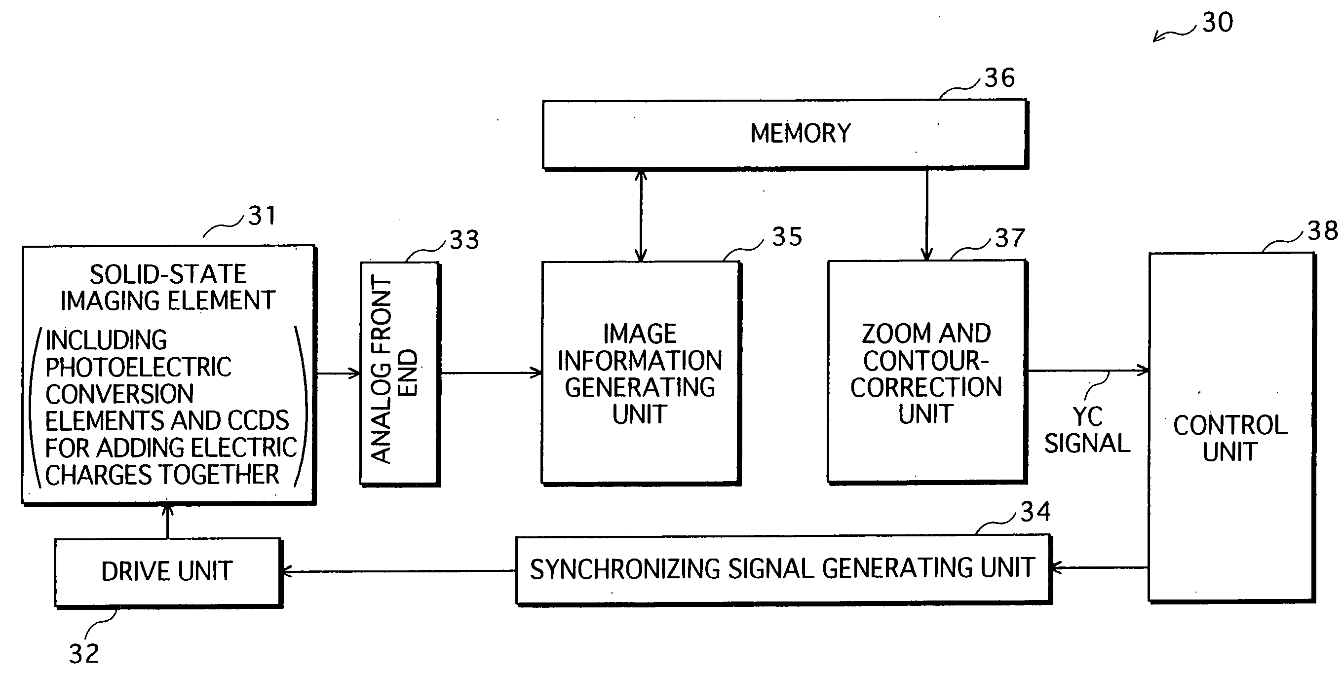
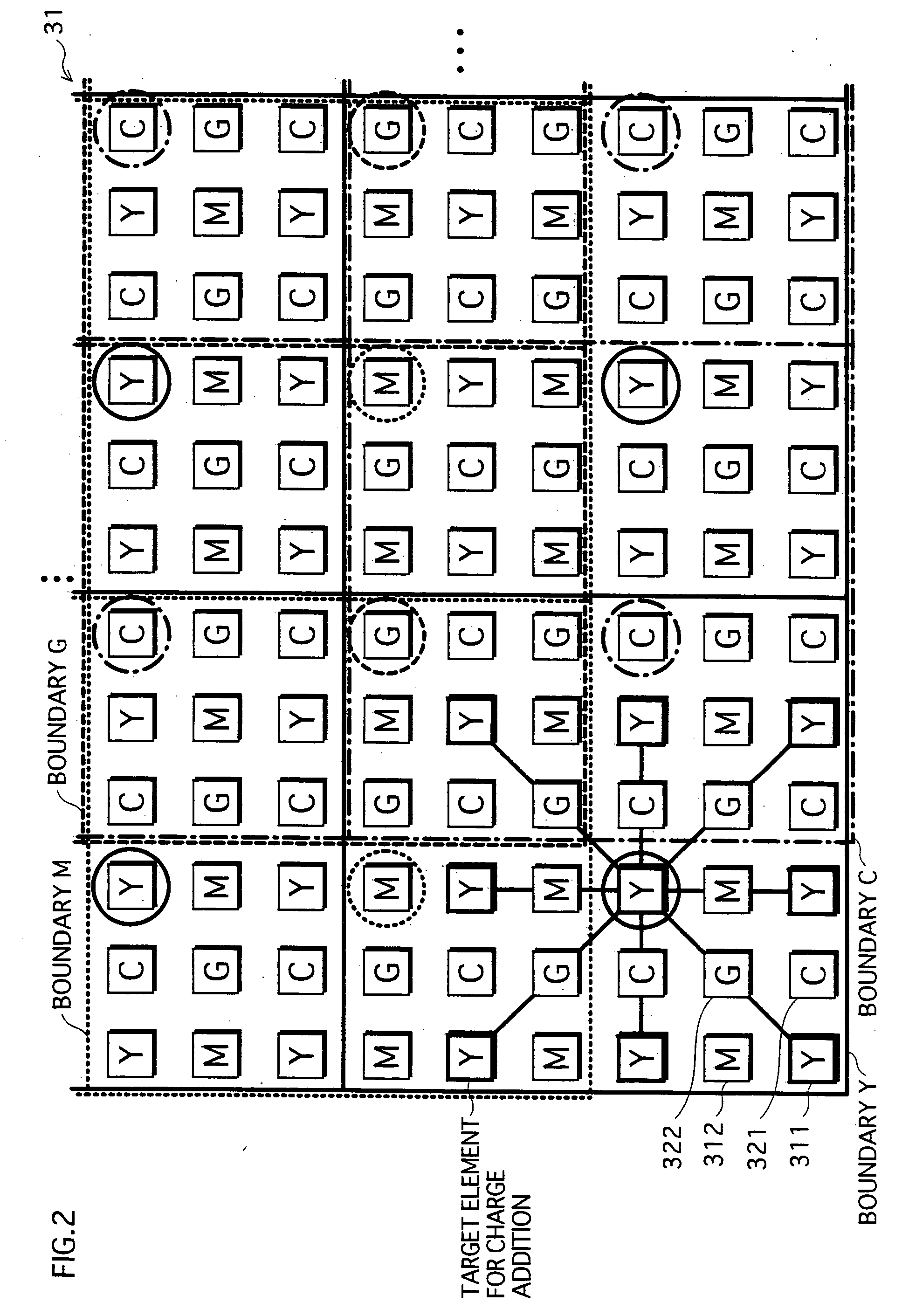
[0032] An imaging device relating to an embodiment of the present invention produces image data showing an image with a target resolution in the following manner. Electric charges stored in each group of the predetermined number of pixels in an solid-state imaging element are added together, to obtain a resulting electric charge. Thus, the solid-state imaging element produces image data showing an image with a tentative resolution which is lower than an original resolution of the solid-state imaging element and higher than the target resolution. In the image with the tentative resolution, each pixel is represented by a resulting electric charge. After this, the solid-state imaging element performs a zoom operation and a contour correction operation on the image data with the tentative resolution, to produce the image data showing the image with the target resolution.

[0033] The following part describes the imaging device relating to the embodiment of the present invention with refer...


PUM


Abstract

A solid-state imaging element includes photoelectric conversion elements having a complementary or Bayer color filter array. The solid-state imaging element adds together electric charges stored in nine photoelectric conversion elements having color filters of one of multiple colors in each portion of six rows and six columns, to obtain a resulting electric charge, and outputs the resulting electric charge as one pixel. A portion for one of the colors deviates from a portion for each of the other colors by three rows and / or three columns. This pixel-addition operation produces an effect of a spatial low pass filter, thereby reducing signal components exceeding a Nyquist frequency corresponding to a target resolution. Consequently, aliasing noise in an image with the target resolution is reduced, and therefore higher image quality can be achieved, when compared with a conventional resolution reduction technique.

Description

BACKGROUND OF THE INVENTION [0001] (1) Field of the Invention [0002] The present invention relates to an imaging device, especially to a technique to produce an image with a resolution lower than an original resolution of the imaging device and excellent image quality. [0003] (2) Description of the Related Art [0004] In recent years, solid-state imaging elements have a larger number of pixels. Solid-state imaging elements with a resolution exceeding megapixel, i.e. one million pixels are now used even in simple devices such as compact cameras and mobile telephones. [0005] Accordingly, still pictures with a very high resolution can be taken with such simple devices. On the other hand, images with a resolution lower than an original resolution of a solid-state imaging element are necessary to be used for individual frame pictures of a moving picture and images to be attached with e-mails. Accordingly, an operation for reducing a resolution has become indispensable. [0006] As a techniq...

Claims


Application Information

Patent Timeline
Patent Type & Authority Applications(United States)
IPC IPC(8): H04N1/387H04N5/262H04N5/335H04N5/357H04N5/369H04N5/372H04N9/04H04N9/07
CPCH04N9/045H04N3/1562H04N25/445H04N25/46H04N25/73H04N23/84H04N25/136H04N1/387H04N5/262
Inventor KAWASAKI, MAKOTOINOKUMA, KAZUYUKIFUJII, TOSHIYA
Owner PANASONIC SEMICON SOLUTIONS CO LTD
Why Eureka
Try Eureka