PLL circuit

Inactive Publication Date: 2005-04-21
RENESAS ELECTRONICS CORP
View PDF5 Cites 1 Cited by
  • Summary
  • Abstract
  • Description
  • Claims
  • Application Information

AI Technical Summary

Benefits of technology

[0011] In the charge pump circuit described in the above Patent Document 1, it is possible to adjust the unbalance between the transistors MP1 and MN1 produced in the form of a DC, caused by the output potential VC. However, in an operating condition in particular in which the transistors MP2 and MN2 are turned on and off only during a short period when the charge pump is actually used, the unbalance that will be described hereinafter is produced. Thus, the effect of reducing the phase offset between input clocks to the phase comparator is restricted.
[0013] In view of the problems encountered by the conventional PLL circuit described above, an object of the present invention is to provide a PLL circuit in which a phase offset caused by a difference in the current driving capability of a charge pump and a phase offset caused by an unbalance among circuit elements in a phase comparator and the PLL circuit can be reduced.
[0018] By using the voltage-controlled delay elements, the pulse widths of the up and down signals can be easily controlled, based on the output of the amplifier. By controlling the amounts of delay of the signals input to the pair of inputs for comparison of the phase comparator and the dummy phase comparator by the voltage-controlled delay elements, the pulse widths of the up and down signals, which are the outputs of the phase comparator, can be controlled.
[0022] According to the PLL circuit of the present invention, not only an unbalance caused by a difference in the current driving capability of the charge pump, but also other unbalance within the charge pump and a phase offset caused by an unbalance in the phase comparator can be reduced. Thus, an output clock signal having a phase well aligned with the phase of the reference clock signal can be generated.

Problems solved by technology

However, in an operating condition in particular in which the transistors MP2 and MN2 are turned on and off only during a short period when the charge pump is actually used, the unbalance that will be described hereinafter is produced.
Thus, the effect of reducing the phase offset between input clocks to the phase comparator is restricted.
Further, even by a difference among the current driving capabilities of the transistors inside the phase comparator as well, the unbalance is produced.

Method used


Image

  • PLL circuit
  • PLL circuit
  • PLL circuit

Examples


first embodiment

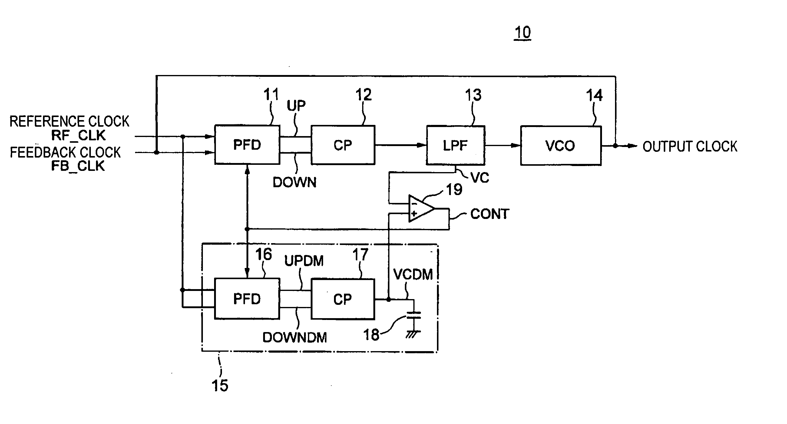
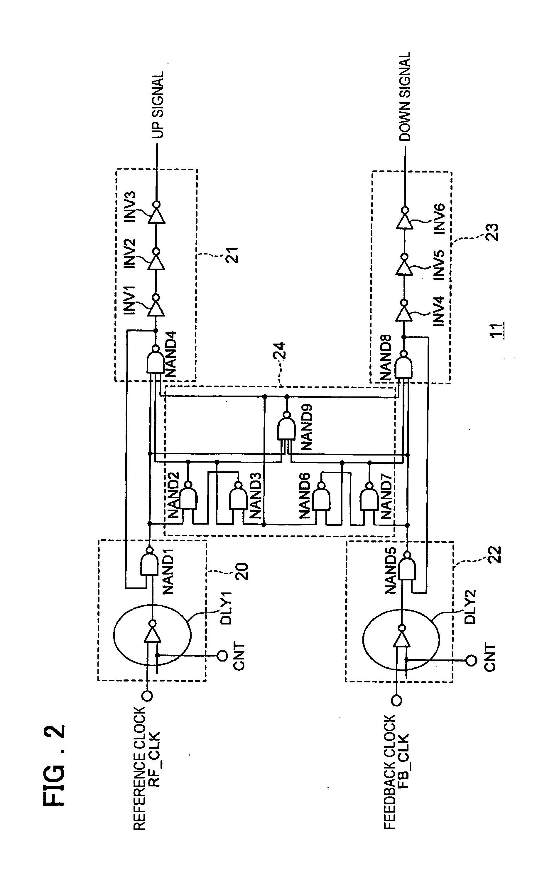
[0032] The present invention will be further described below, based on the embodiments thereof, with reference to the appended drawings. FIG. 1 shows a configuration of a PLL circuit according to the present invention. A PLL circuit 10 includes a phase comparator 11, a charge pump 12, a low-pass filter 13, and a voltage-controlled oscillator 14 that constitutes the same loop as in the prior art, an unbalance adjusting circuit block 15, and an operational amplifier 19 for comparing the output voltage of the loss pass filter 13 that constitutes the loop with the output voltage of the unbalance adjusting circuit block 15 to generate a control voltage signal CONT.

[0033] The unbalance adjusting circuit block 15 includes a dummy phase comparator 16 and a dummy charge pump 17, and a capacitor 18 for removing high frequency components from the output voltage VCDM of the dummy charge pump 17. By having same circuit configurations and device dimensions as the phase comparator 11 and the charg...

second embodiment

[0045]FIG. 5 shows a configuration of a phase comparator 11A of a PLL circuit according to the present invention. The PLL circuit in this embodiment has the same configuration as the PLL circuit shown in FIG. 1, except for the configurations of the phase comparator and the dummy phase comparator. The dummy phase comparator in this embodiment has the same configuration as the phase comparator 11A shown in FIG. 5, except that a pair of inputs for comparison is connected in common and the reference clock signal is input to the inputs for comparison.

[0046] The phase comparator 11A includes a reference clock signal input unit 25 for inputting the reference clock signal, an UP signal generating unit 26 for generating the UP signal, a feedback clock signal input unit 27 for inputting the feedback clock signal, a DOWN signal generating unit 28 for generating the DOWN signal, and a reset signal generating unit 29 for generating the reset signal.

[0047] The reference clock signal input unit 2...


PUM


Abstract

A PLL circuit in which a phase offset between a reference clock and a feedback clock is reduced. PLL circuit 10 includes a dummy phase comparator 16 that simulates a phase comparator 11 and has a pair of comparison inputs to which the reference clock is input, a dummy charge pump 17 that simulates a charge pump 12 and causes an output voltage thereof to rise or fall based on an up signal or a down signal output from the dummy phase comparator 16, and an amplifier 19 for detecting a difference between the output voltage of the charge pump 12 and the output voltage of the dummy charge pump 17. The PLL circuit controls the pulse widths of up and down signals of both of the phase comparator 11 and the dummy phase comparator 16 based on the output voltage of the amplifier 19.

Description

FIELD OF THE INVENTION [0001] The present invention relates to a PLL circuit. More specifically, the invention relates to a PLL circuit in which a phase offset between a reference clock signal and a feedback clock signal is reduced. BACKGROUND OF THE INVENTION [0002] PLL circuits are extensively used in various electronic circuits as the circuits for generating an internal clock signal synchronized with an input reference clock signal. FIG. 7 shows a conventional common PLL circuit using a block diagram. A PLL circuit 30 includes a phase comparator 31, a charge pump 32, a low-pass filter 33, and a voltage-controlled oscillator 34. By feed backing the output of the voltage-controlled oscillator 34 to the phase comparator 31, these are connected to a loop. The phase comparator 31 compares the phase of a reference clock signal RF_CLK with the phase of a feedback clock signal FB_CLK to each other, and generates an UP signal or a DOWN signal, which is a phase difference signal, based on ...

Claims


Application Information

Patent Timeline
IPC IPC(8): H03L7/08H03L7/00H03L7/087H03L7/089
CPCH03L7/0891H03L7/087
Inventor HASEGAWA, ATSUSHI
Owner RENESAS ELECTRONICS CORP
Why Eureka
Try Eureka