High-frequency signal transmitting device
a high-frequency signal and transmitting device technology, applied in the direction of waveguide type devices, high-frequency circuit adaptations, printed circuit aspects, etc., can solve the problem that the high-frequency transmission characteristic of the high-frequency signal transmitting device having the conventional construction is not good, and achieve good high-frequency transmission characteristics
- Summary
- Abstract
- Description
- Claims
- Application Information
AI Technical Summary
Benefits of technology
Problems solved by technology
Method used
Image

Examples
example 4
(EXAMPLE 4)
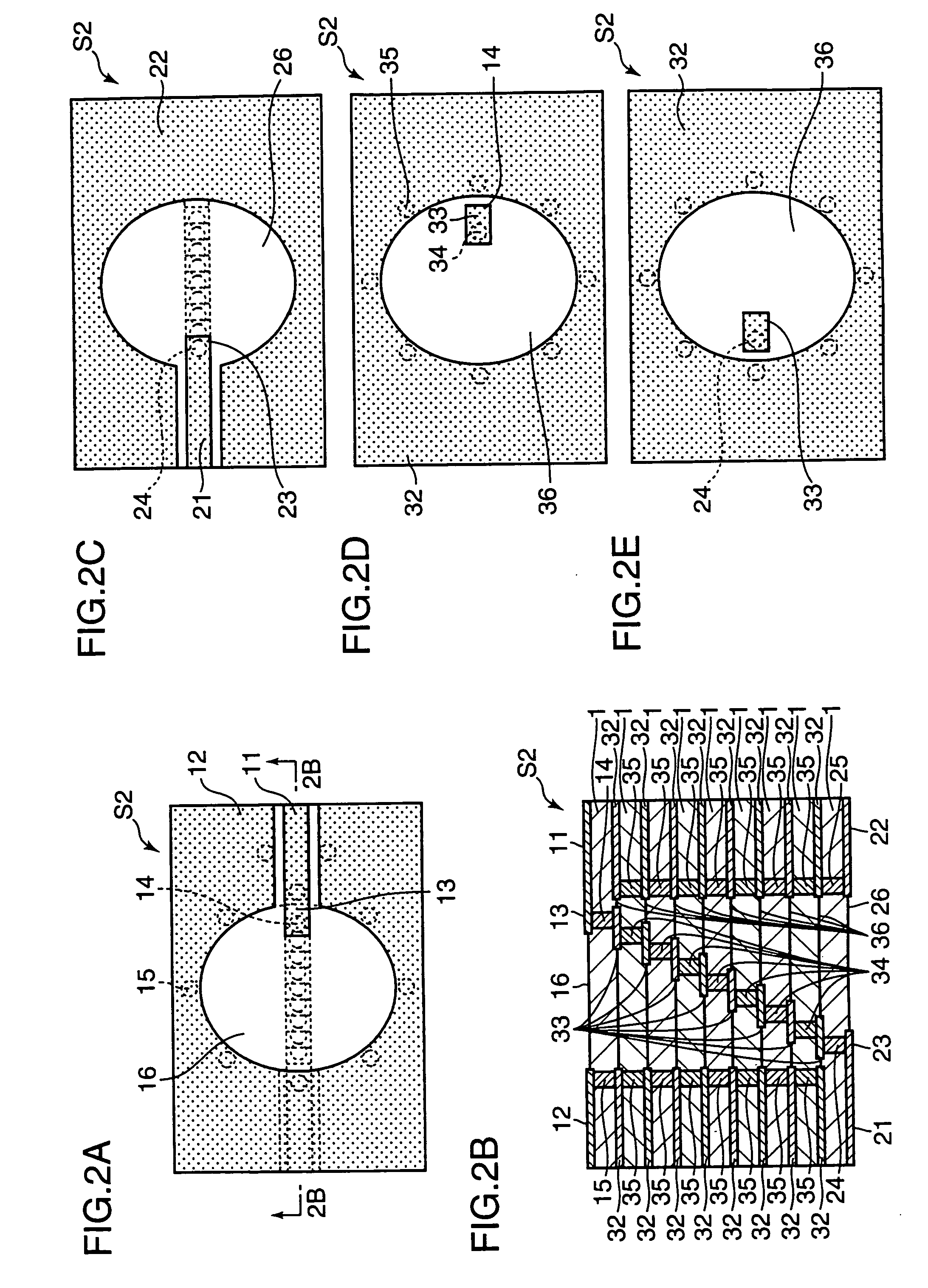
[0361] The high-frequency signal transmitting device S6 having the construction shown in FIGS. 6A to 6C was formed by defining the rectangular grounding-conductor non-forming areas 36 such that the longer sides thereof (lengths in a direction perpendicular to the signal wiring conductors 11, 21) were 1.0 mm and the shorter sides thereof (lengths in a direction along the signal wiring conductors 11, 21) were 0.68 mm, 0.76 mm, 0.84 mm, 0.92 mm, 0.92 mm, 0.84 mm, 0.76 mm, 0.68 mm from top. A sample T6 was obtained by setting the other construction as in the sample T4. In other words, the sample T6 was such that the shorter sides of the grounding-conductor non-forming areas 36 were made longer by the same length between the respective dielectric layers 1 from the upper layers toward the middle layers and from the lower layers toward the middle layers.
[0362] The high-frequency signal transmitting device S7 having the construction shown in FIGS. 7A to 7C was formed by defining...
example 5
(EXAMPLE 5)
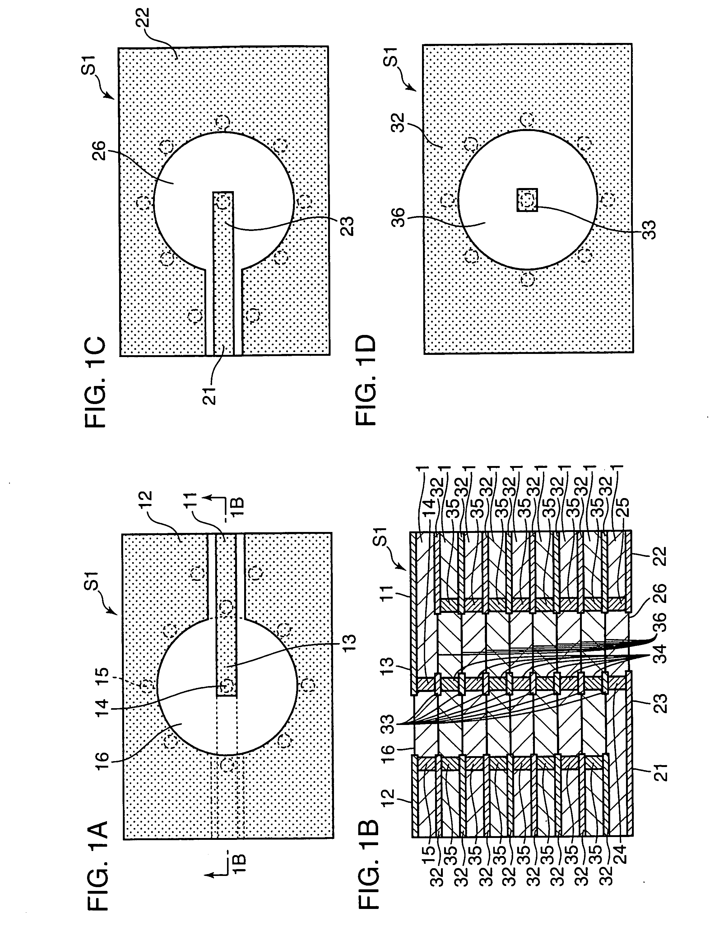
[0364] The high-frequency signal transmitting device S8 having the construction shown in FIGS. 8A to 8C was formed by defining the grounding-conductor non-forming area 16 on the upper surface of the uppermost dielectric layer 1, the grounding-conductor non-forming area 36 on the upper surface of the uppermost intermediate dielectric layer 1 and the grounding-conductor non-forming area 26 on the lower surface of the bottommost dielectric layer 1 such that the diameter thereof was 0.46 mm and defining the grounding-conductor non-forming areas 36 of the other dielectric layers 1 such that the diameter thereof was 1.0 mm. A sample T8 was obtained by setting the other construction as in the sample T1.
[0365] For this sample T8, a high-frequency characteristic between the edges of the signal wiring conductors 11, 21 was measured by an electromagnetic field simulation to obtain a characteristic curve having a frequency characteristic as shown in a graph of FIG. 35. As is clear f...
example 6
(EXAMPLE 6)
[0366] The high-frequency signal transmitting device S9 having the construction shown in FIGS. 9A to 9C was formed by setting the widths of the signal-wiring connecting conductors 13, 23 of the uppermost and bottommost dielectric layers 1 to 0.22 mm. A sample T9 was obtained by setting the other construction as in the sample T3.
[0367] For this sample T9, a high-frequency characteristic between the edges of the signal wiring conductors 11, 21 was measured by an electromagnetic field simulation to obtain a characteristic curve having a frequency characteristic as shown in a graph of FIG. 36. As is clear from FIG. 36, the sample T9 which is the high-frequency signal transmitting device according to the present invention can be understood to possess a good electrical characteristic by having less reflection even in a high-frequency band. It should be noted that the characteristic curve of the sample T3 which is the high-frequency signal transmitting device according to the p...
PUM
 Abstract
Description
Claims
Application Information
 - R&D
- Intellectual Property
- Life Sciences
- Materials
- Tech Scout
- Unparalleled Data Quality
- Higher Quality Content
- 60% Fewer Hallucinations
Browse by: Latest US Patents, China's latest patents, Technical Efficacy Thesaurus, Application Domain, Technology Topic, Popular Technical Reports.
© 2025 PatSnap. All rights reserved.Legal|Privacy policy|Modern Slavery Act Transparency Statement|Sitemap|About US| Contact US: help@patsnap.com