Apparatus and method for improved wafer transport ambient

a technology of ambient and apparatus, applied in the direction of packaging, loading/unloading, furniture, etc., can solve the problem of low final yield of good semiconductor products, and achieve the effect of preventing or reducing the introduction of external particles

Inactive Publication Date: 2005-05-26
SAMSUNG ELECTRONICS CO LTD
View PDF14 Cites 50 Cited by
  • Summary
  • Abstract
  • Description
  • Claims
  • Application Information

AI Technical Summary

Benefits of technology

[0010] A filter for preventing or reducing the introduction of external particles into the container and an inflow hole open / close assembly for opening / closing the inflow hole may be inserted into the inflow hole. The inflow hole open / close assembly includes a fixture that is coupled to the flow hole and protrudes inwardly toward the inflow hole, an isolation plate for opening / closing a flow path through the fixture, and an elastic body connected to the isolation plate an arranged to apply force to the isolation plate tending to maintain a closed position. A passage for the gas may be provided at the center of the fixture. The isolation plate may be moved within the fixture by the pressure of the gas supplied from the injection part.

Problems solved by technology

Thus, these contaminants will be present in the sealed FOUP and may oxidize a wafer surface or bind to the wafer surface in a manner that can interfere with subsequent processing or otherwise lower the final yield of good semiconductor products.

Method used


Image

  • Apparatus and method for improved wafer transport ambient
  • Apparatus and method for improved wafer transport ambient
  • Apparatus and method for improved wafer transport ambient

Examples


Embodiment Construction

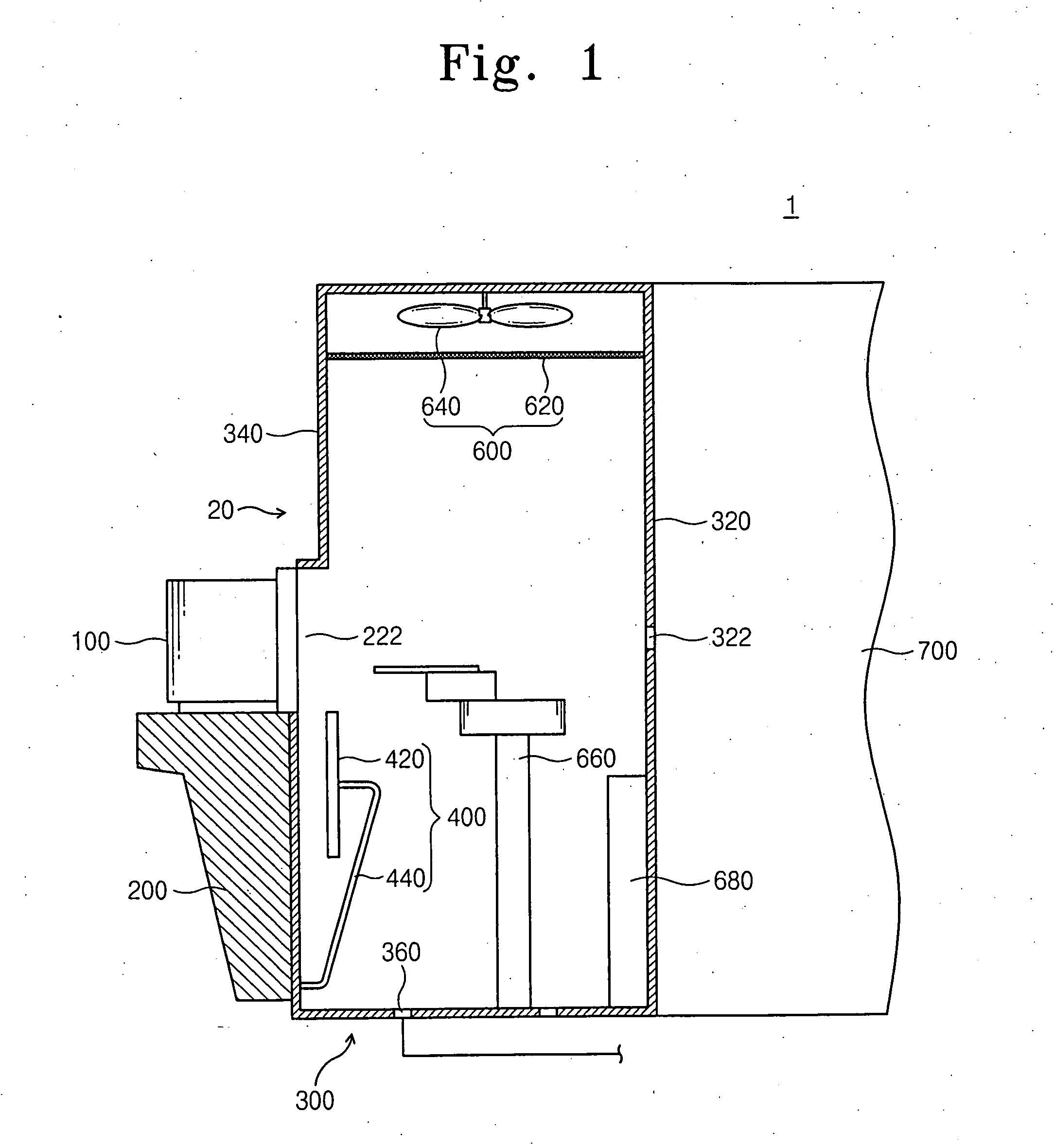
[0032] As illustrated in FIG. 1, a substrate treating or processing device 1 includes a container 100, a wafer handling system 20, and a purge part (500 of FIG. 5). The container 100 is a receptacle configured for receiving semiconductor substrates such as silicon wafers and will typically be a front open unified pod (hereinafter referred to as “FOUP”). The FOUP is a sealable wafer carrier used for shielding wafers from atmospheric and / or chemical contamination while transferring wafers between processing equipment and or storage areas.

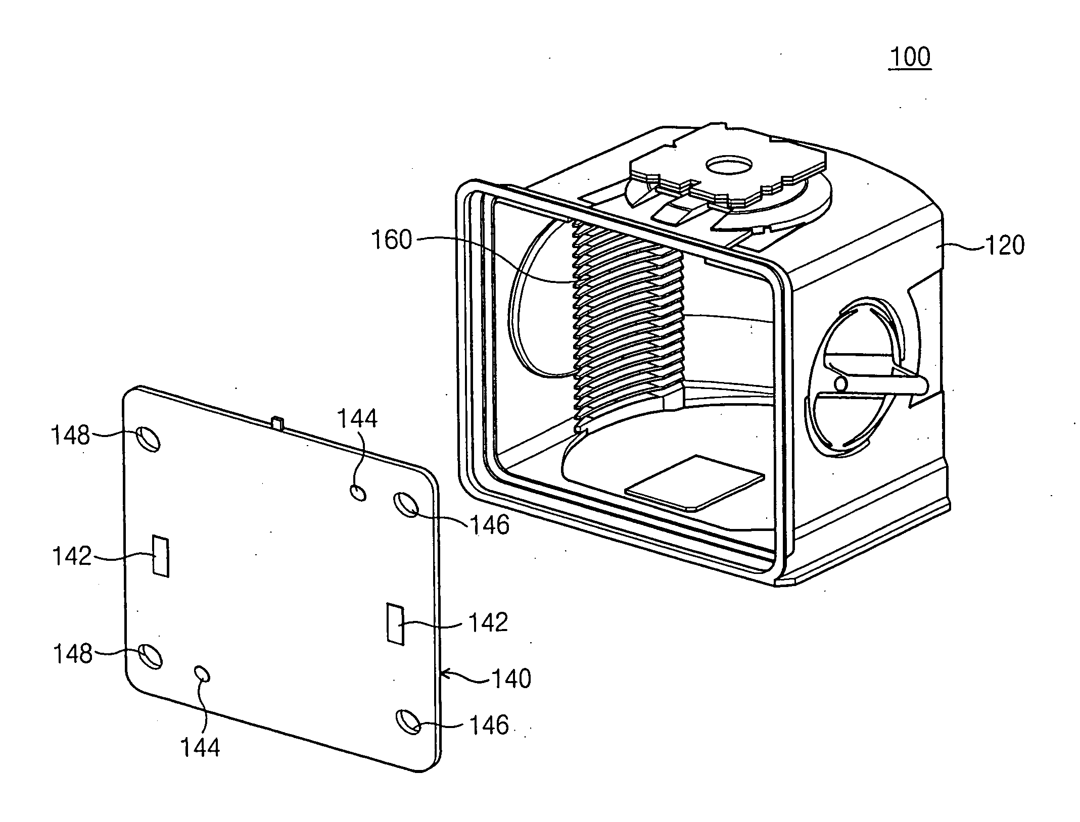
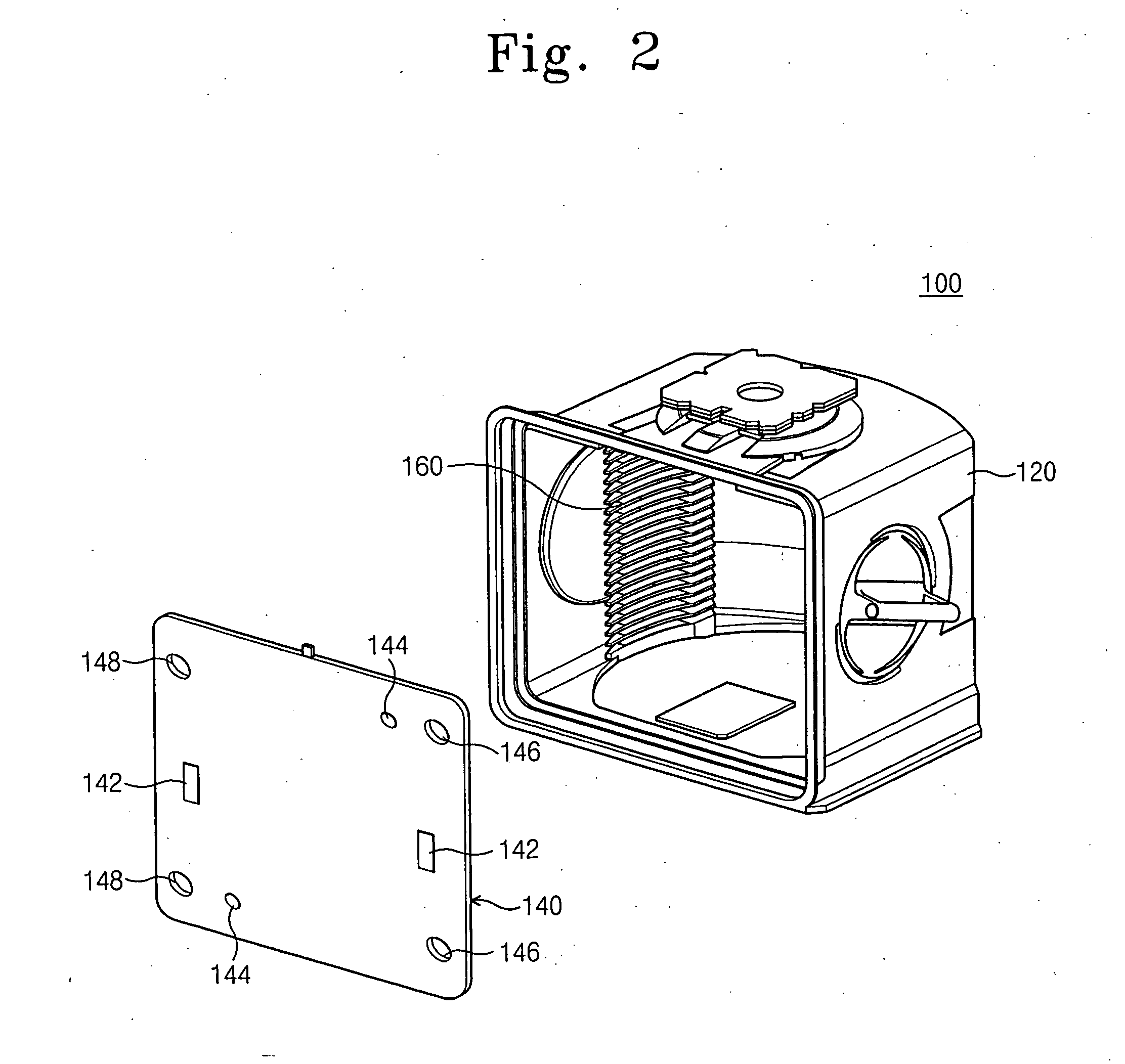
[0033] As illustrated in FIG. 2, the FOUP 100 may include a front-opening body 120 and a door 140 for opening / closing the front of the body 120. Parallel slots 160 are typically formed on the inner walls of the body 120 for supporting and separating wafers within the FOUP. The slots 160 may be substantially perpendicular to a plane defined by the door 140.

[0034] The wafer handling system 20 can be used to transfer wafers from the FOUP 100 to the pro...


PUM


Abstract

An improved wafer transfer apparatus is provided that allows the ambient atmosphere within a modified front open unified pod (“FOUP”) while the FOUP is positioned on a loading stage provided on an equipment front end module (“EFEM”). In particular, the wafer transfer apparatus includes both an injection assembly and an exhaust assembly that will be engaged when the door of the FOUP is docked to a door holder provided on the EFEM. The injection assembly may include a mass flow controller (“MFC”) for controlling the injection of purge gas(es) into the container. Similarly, the exhaust assembly may include a MFC for controlling the removal of fluid from the container. While the door is docked to the door holder, inert or less reactive gases may be introduced into the container, thereby reducing the likelihood of oxidation or contamination of the wafers therein.

Description

CROSS REFERENCE TO RELATED APPLICATIONS [0001] This U.S. nonprovisional patent application claims priority under 35 U.S.C. § 119 from Korean Patent Application 2003-79859, which was filed on Nov. 12, 2003, the entire contents of which are hereby incorporated by reference. BACKGROUND OF THE INVENTION [0002] 1. Field of the Invention [0003] The present invention relates to apparatus and method for transporting semiconductor substrates within a clean room and delivering wafers to and receiving wafers from automated process equipment and, more particularly, to an apparatus including a load port for opening / closing a door provided on a container in which semiconductor substrates are loaded and a method for filling the inside of the container with a selected gas or gas mixture to improve the ambient environment to which the wafers are exposed during transport and storage. [0004] 2. Discussion of the Related Art [0005] Conventional semiconductor manufacturing processes are performed in lar...

Claims


Application Information

Patent Timeline
Patent Type & Authority Applications(United States)
IPC IPC(8): B65D85/86B65G49/00H01L21/00H01L21/673H01L21/677H01L21/68
CPCH01L21/67017H01L21/67775H01L21/67772H01L21/68
Inventor KIM, HYEOG-KILEE, KUN-HYUNGLEE, OK-SUNKIM, KI-DOOCHO, CHANG-MIN
Owner SAMSUNG ELECTRONICS CO LTD
Why Eureka
Try Eureka