Memory circuit with shared redundancy

a memory circuit and redundancy technology, applied in the field of memory, can solve problems such as affecting the performance of memory circuits, and achieve the effect of less integrated circuit surface area

Inactive Publication Date: 2005-07-07
STMICROELECTRONICS SRL
View PDF5 Cites 0 Cited by
  • Summary
  • Abstract
  • Description
  • Claims
  • Application Information

AI Technical Summary

Benefits of technology

[0022] The present invention thus aims at providing a solution which consumes less integrated circuit surface area.

Problems solved by technology

However, a major disadvantage of such a solution is that it considerably increases the memory circuit size.

Method used


Image

  • Memory circuit with shared redundancy
  • Memory circuit with shared redundancy
  • Memory circuit with shared redundancy

Examples


Embodiment Construction

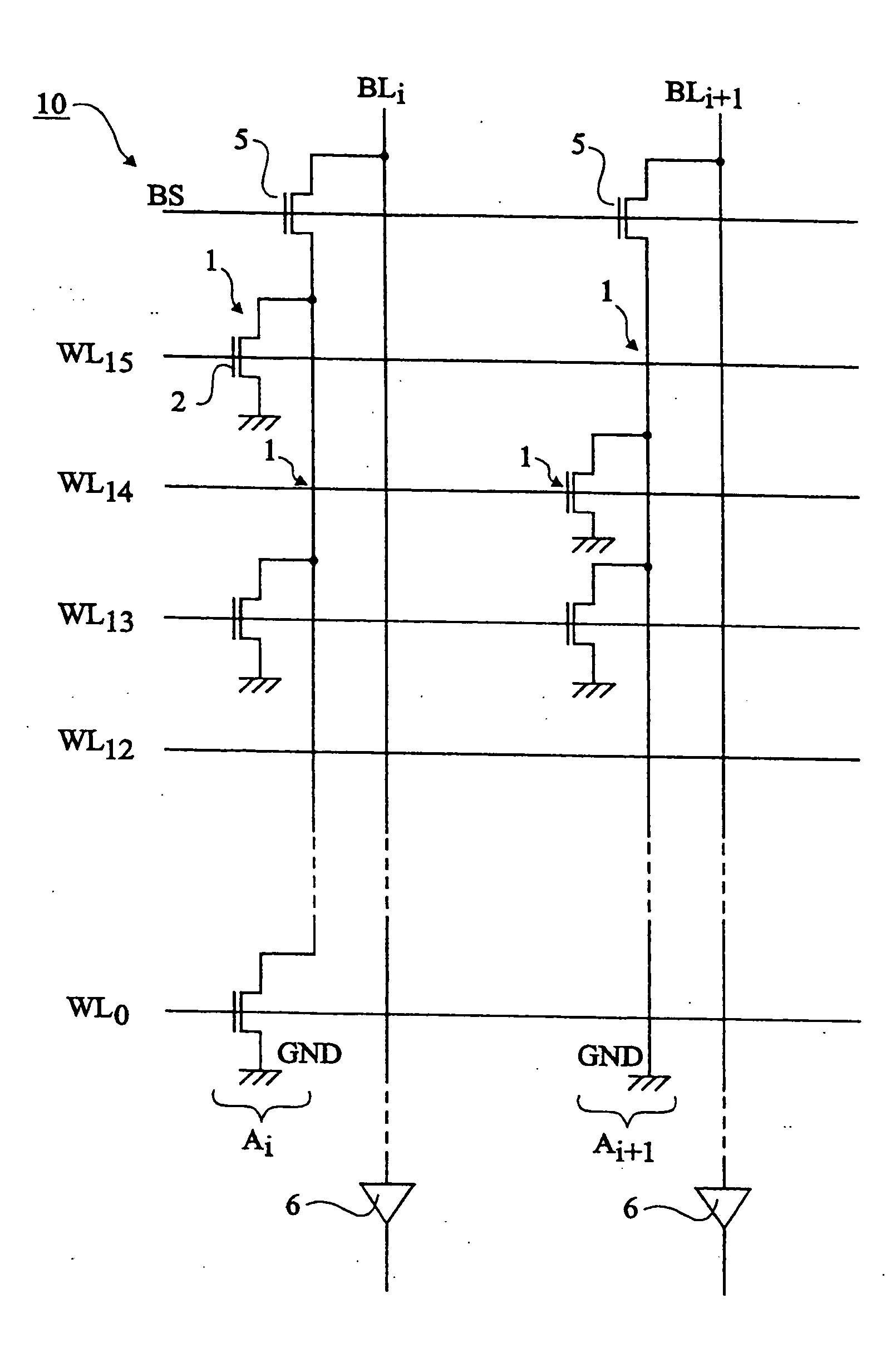
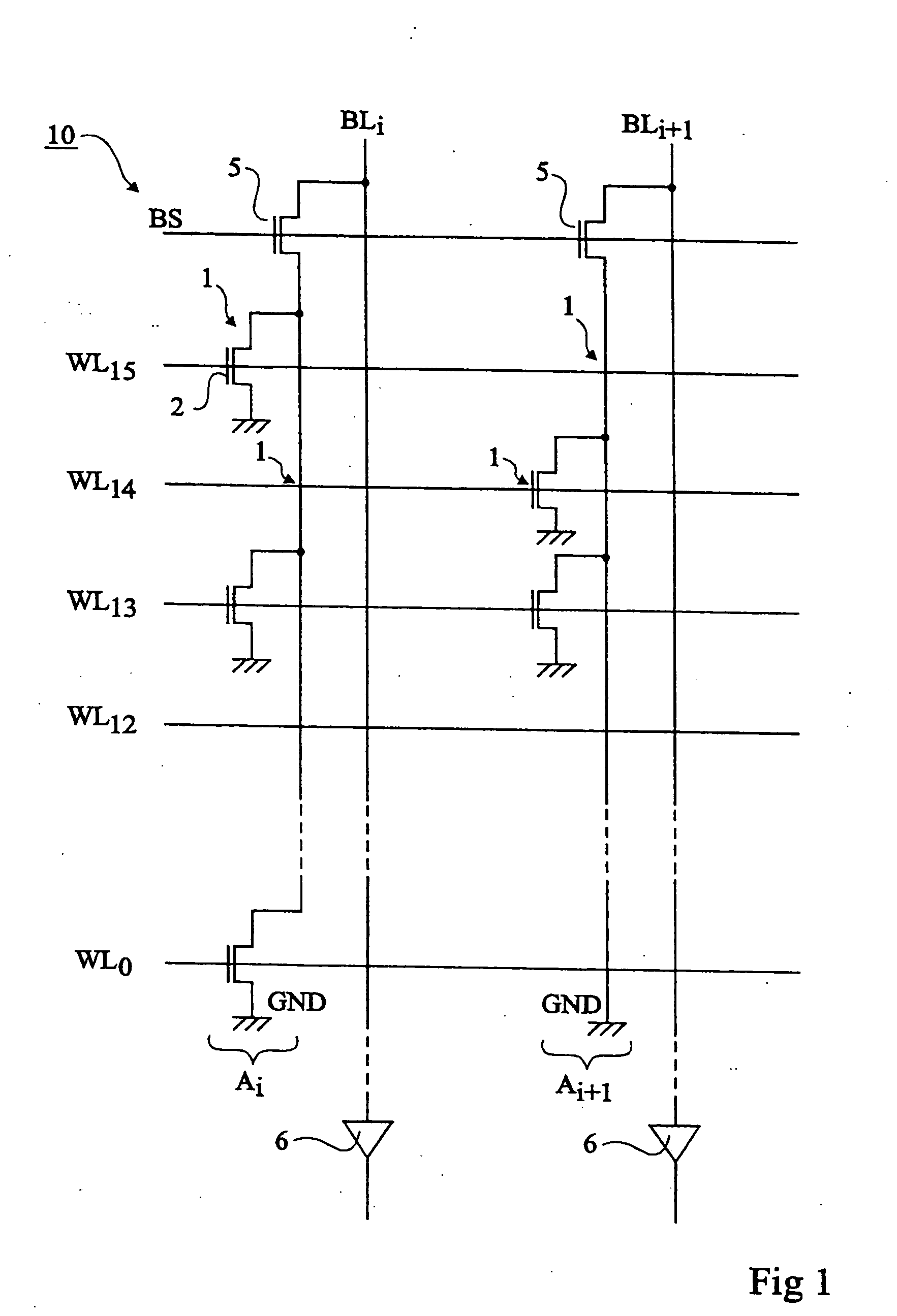
[0039] The same elements have been designated with the same references in the different drawings. For clarity, only those elements which are necessary to the understanding of the present invention have been shown in the drawings and will be described hereafter. In particular, the details constitutive of the memory banks, of the sense amplifiers, of the input / output buffers, and of the decoding and addressing circuits have not been detailed.

[0040] A feature of the present invention is to place, at the level of each memory bank, that is, at the level of each cell array associated with a sense amplifier row, a circuit for reorganizing or reassigning the columns. This circuit enables individualizing, at the level of each memory bank, the use of the redundancy column(s).

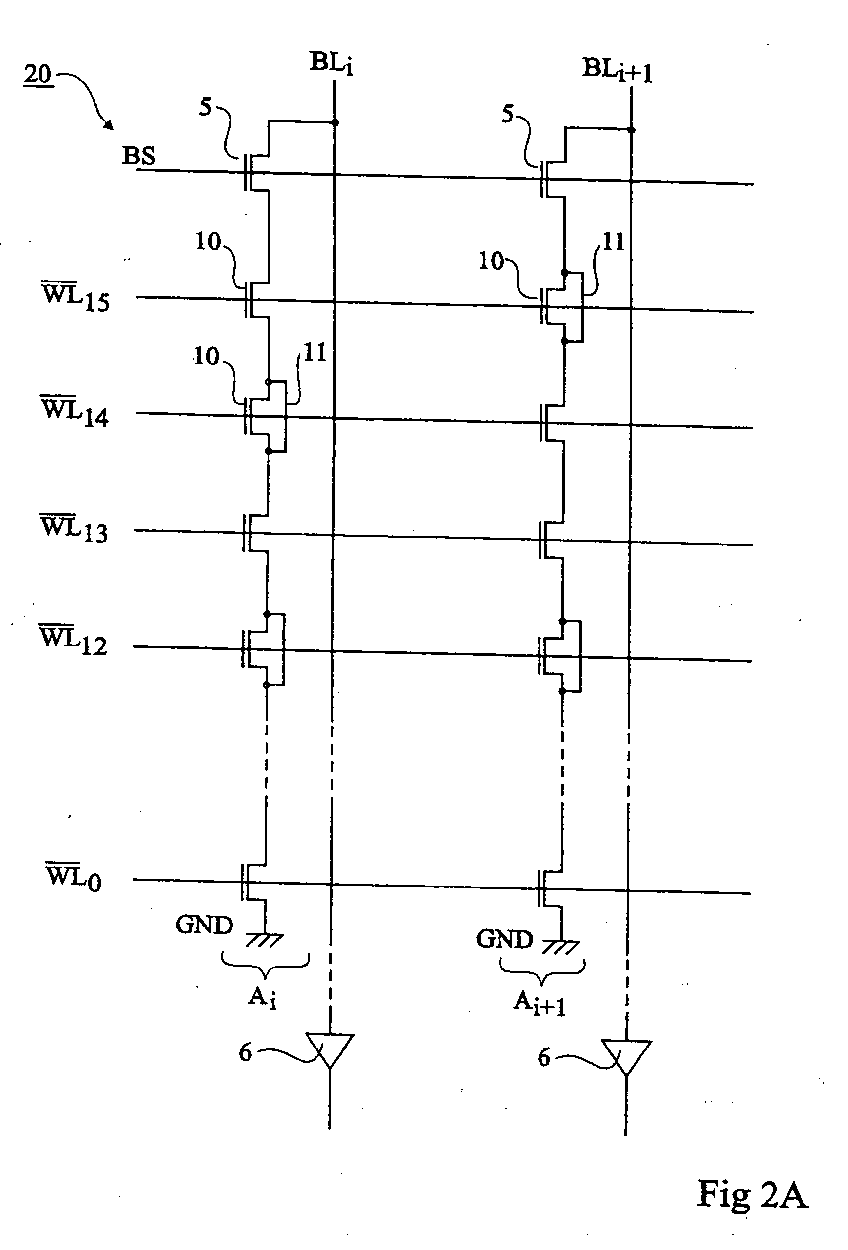
[0041]FIG. 2 shows, in a very simplified top view to be compared with that of FIG. 1, an embodiment of a memory circuit architecture according to the present invention.

[0042] As previously, several banks Bl, Bk, Bp−1, ...


PUM


Abstract

An integrated circuit memory including at least two banks each provided with an array of storage elements having at least one redundancy column and each associated with specific sense amplifiers, a row of input/output buffer circuits common to the memory banks, and for each memory bank, a circuit for assigning the redundancy column to an input/output line connected to one of said buffers. The assigning can be performed, for a line of current rank, towards the columns of preceding rank and towards the columns of following rank.

Description

[0001] This application is a continuation of prior application Ser. No. 10 / 630,236, filed Jul. 30, 2003 which in turn is a continuation of prior application Ser. No. 10 / 328,712, filed Dec. 23, 2002, which in turn is a continuation of prior application Ser. No. 10 / 197,229, filed on Jul. 17, 2002 which in turn is a continuation of prior application Ser. No. 10 / 010,744, filed on Dec. 7, 2001, entitled MEMORY CIRCUIT WITH SHARED REDUNDANCY.BACKGROUND OF THE INVENTION [0002] 1. Field of the Invention [0003] The present invention relates to memories formed in integrated circuits and provided with redundancy elements. [0004] The present invention more specifically relates to integrated circuit memories formed of several arrays provided with amplifiers for reading the memory cells of each network and sharing common input / output circuits. [0005] 2. Discussion of the Related Art [0006] The function of redundancy elements is to increase the manufacturing output of integrated circuit memories b...

Claims


Application Information

Patent Timeline
Patent Type & Authority Applications(United States)
IPC IPC(8): G06F11/20G11C7/00G11C29/00
CPCG11C29/848G11C29/808
Inventor FERRANT, RICHARDJACQUET, FRANCOISMURILLO, LAURENT
Owner STMICROELECTRONICS SRL
Why Eureka
Try Eureka