Methods, systems, and apparatus for uniform chemical-vapor depositions

a chemical vapor deposition and uniform technology, applied in the field of integrated circuit making, can solve the problems of non-uniform thickness, increasing difficulty, if not completely impracticality, to overcome the non-uniform thickness of conventional cvd layers, etc., and achieves the effects of less gas consumption, less cvd, and less cvd

Inactive Publication Date: 2005-02-08
MICRON TECH INC
View PDF276 Cites 149 Cited by
  • Summary
  • Abstract
  • Description
  • Claims
  • Application Information

AI Technical Summary

Benefits of technology

The inner chamber has a smaller volume than the outer chamber and thus consumes less gas during the deposition process than would the outer chamber used alone. Also, the smaller chamber volume allows the exhaust system to pump the chamber more quickly, thus increasing the rate of the CVD process. In addition, the exemplary showerhead is made of a material, like silicon, which can be easily passivated to reduce reaction with reactive gases, thus reducing chemical-vapor buildup in the showerhead. Also, the exemplary showerhead includes a configuration of holes that permits uniform gas flow.

Problems solved by technology

Conventional chemical-vapor-deposition (CVD) systems suffer from at least two problems.
First, conventional CVD systems generally form layers that include microscopic hills and valleys and thus have non-uniform thickness.
However, escalating demands for greater circuit density, for thinner layers, and for larger substrates make it increasingly difficult, if not completely impractical, to overcome the non-uniform thickness of conventional CVD layers.
Second, some conventional CVD systems are also inefficient and time consuming.
One significant factor affecting both CVD efficiency and duration is the size of conventional reaction chambers, which are generally made large to allow a loading mechanism to insert and extract the substrate.
However, much of this gas is not only unnecessary based on the amount of material deposited, but is typically treated as waste.
Moreover, large chambers also take longer to fill up or pump out, prolonging deposition cycles and thus slowing fabrication of integrated circuits.

Method used


Image

  • Methods, systems, and apparatus for uniform chemical-vapor depositions
  • Methods, systems, and apparatus for uniform chemical-vapor depositions
  • Methods, systems, and apparatus for uniform chemical-vapor depositions

Examples


Embodiment Construction

following detailed description, which references and incorporates FIGS. 1-4, describes and illustrates specific embodiments of the invention. These embodiments, offered not to limit but only to exemplify and teach the invention, are shown and described in sufficient detail to enable those skilled in the art to make and use the invention. Thus, where appropriate to avoid obscuring the invention, the description may omit certain information known to those of skill in the art.

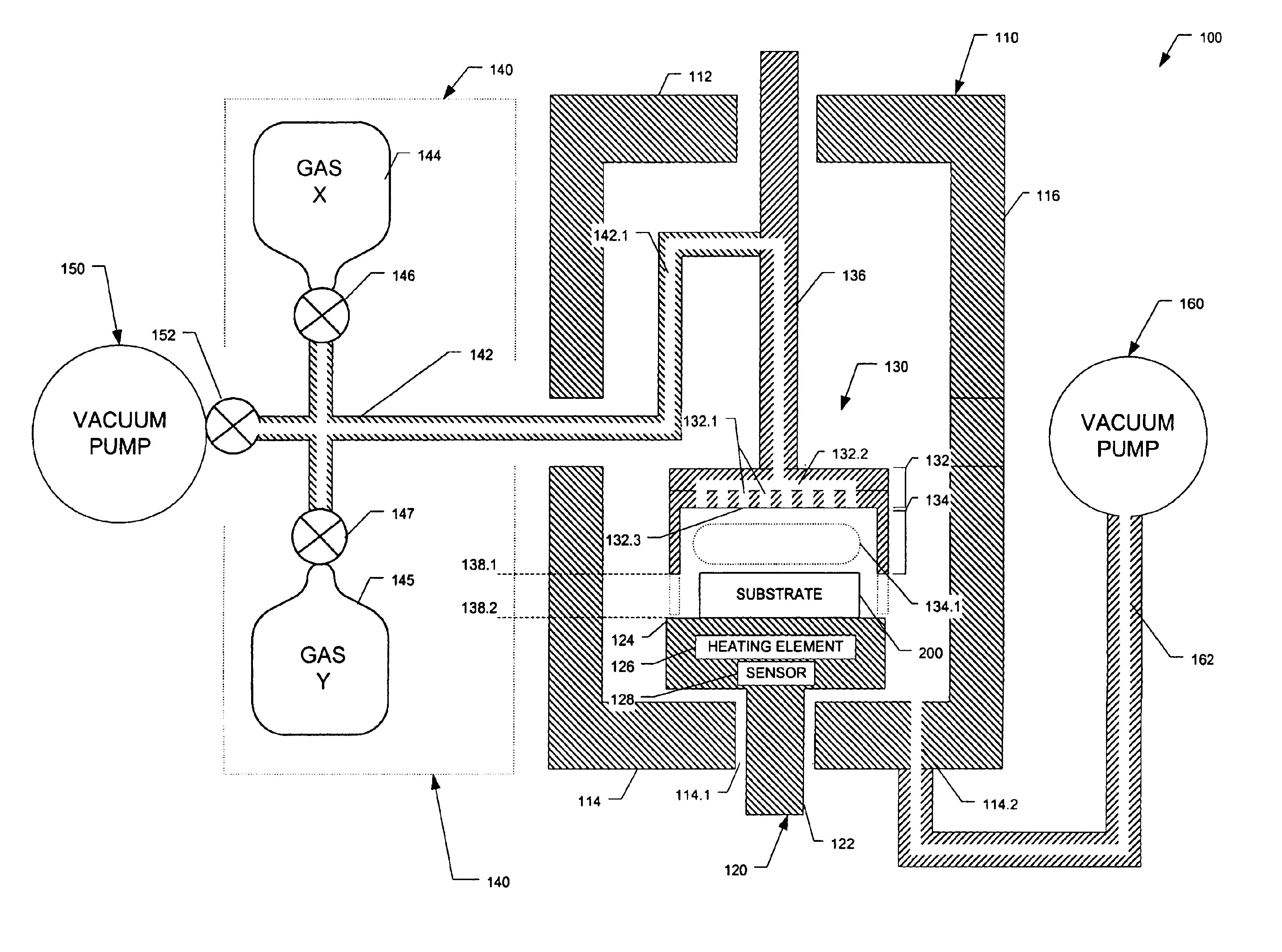
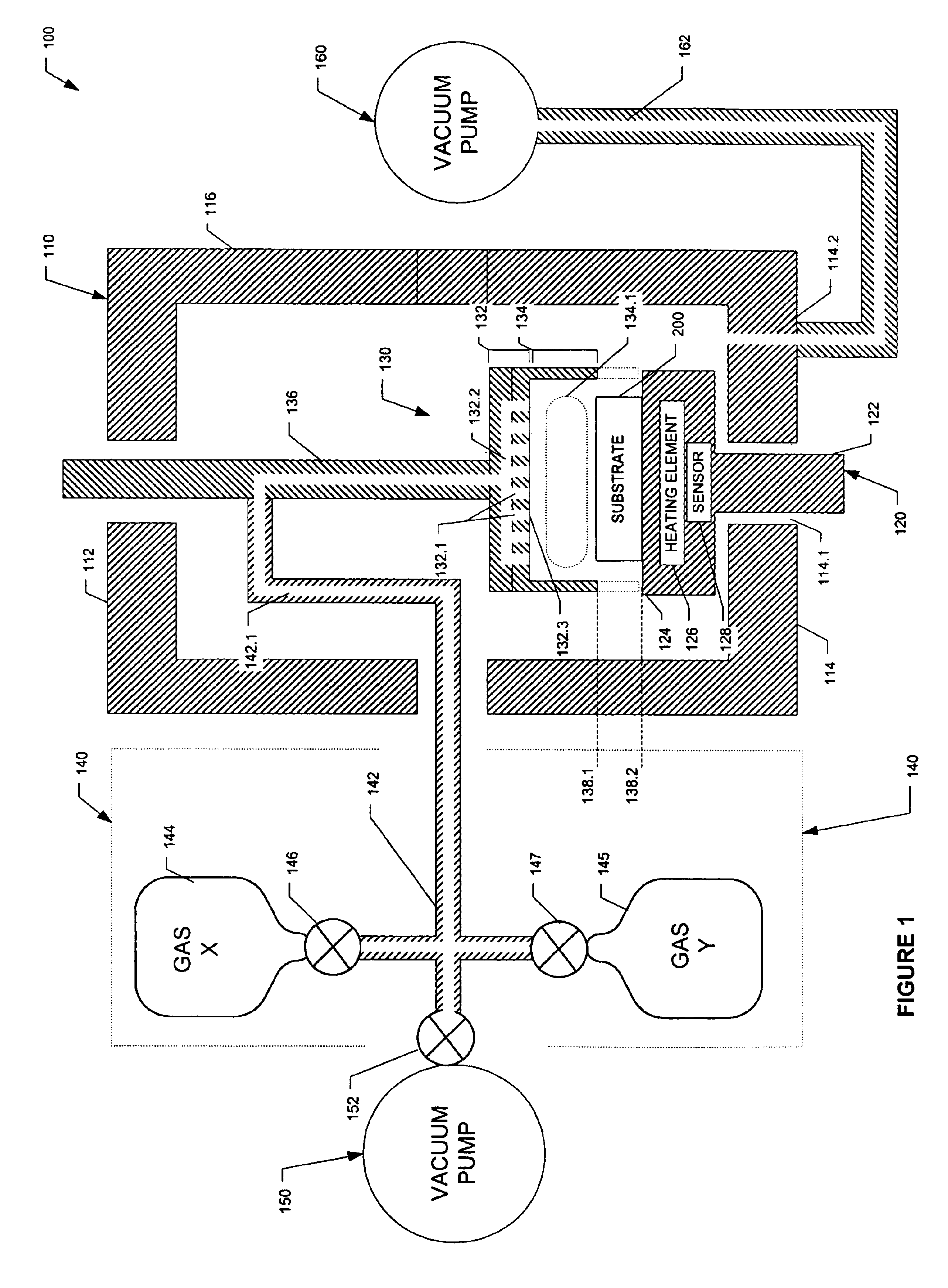
FIG. 1 shows an exemplary chemical-vapor-deposition system 100 which incorporates teachings of the present invention. In particular, system 100 includes a chamber 110, a wafer holder 120, a gas-distribution fixture 130, a gas supply system 140, and exhaust pump 150, and a exhaust pump 160.

More particularly, chamber 110 includes respective top and bottom plates 112 and 114 and a sidewall 116. In the exemplary embodiment, chamber 110 is a cylindrical structure formed of stainless steel or glass. However, other embod...


PUM

PropertyMeasurementUnit
volumeaaaaaaaaaa
diameteraaaaaaaaaa
widthaaaaaaaaaa

Abstract

Integrated circuits, the key components in thousands of electronic and computer products, are generally built layer by layer on a silicon substrate. One common technique for forming layers is called chemical-vapor deposition (CVD.) Conventional CVD systems not only form layers that have non-uniform thickness, but also have large chambers that make the CVD process wasteful and slow. Accordingly, the inventor devised new CVD systems, methods, and apparatuses. One exemplary CVD system includes an outer chamber, a substrate holder, and a unique gas-distribution fixture. The fixture includes a gas-distribution surface having holes for dispensing a gas and a gas-confinement member that engages or cooperates with the substrate holder to form an inner chamber within the outer chamber. The inner chamber has a smaller volume than the outer chamber, which not only facilitates depositions of more uniform thickness, but also saves gas and speeds up the deposition process.

Description

TECHNICAL FIELDThis invention concerns methods of making integrated circuits, particularly layer-formation, such as chemical-vapor deposition.BACKGROUND OF THE INVENTIONIntegrated circuits, the key components in thousands of electronic and computer products, are interconnected networks of electrical components fabricated on a common foundation, or substrate. Fabricators generally build these circuits layer by layer, using techniques, such as deposition, doping, masking, and etching, to form thousands and even millions of microscopic resistors, transistors, and other electrical components on a silicon substrate, known as a wafer. The components are then wired, or interconnected, together to define a specific electric circuit, such as a computer memory.One common technique for forming layers in an integrated circuit is called chemical vapor deposition. Chemical vapor deposition generally entails placing a substrate in a reaction chamber, heating the substrate to prescribed temperature...

Claims


Application Information

Patent Timeline
Patent Type & Authority Patents(United States)
IPC IPC(8): C23C16/455C23C16/44
CPCC23C16/45525C23C16/45544C23C16/45591C23C16/45589C23C16/45565
Inventor AHN, KIE Y.
Owner MICRON TECH INC
Why Eureka
Try Eureka