Method of forming fin field effect transistor

a technology of field effect transistor and fin, which is applied in the direction of transistors, semiconductor devices, electrical equipment, etc., can solve the problems of difficult to electrically isolate individual finfets, difficult to form finfets from soi substrates, and high cost of soi substrates compared with bulk substrates, so as to reduce the amount of etching in the separation of gate electrodes, prevent or substantially reduce leakage current, and reduce the effect of etching

Active Publication Date: 2005-07-14
SAMSUNG ELECTRONICS CO LTD
View PDF6 Cites 394 Cited by
  • Summary
  • Abstract
  • Description
  • Claims
  • Application Information

AI Technical Summary

Benefits of technology

[0014] Some embodiments of the invention provide a method of forming a finFET that may prevent or substantially reduce a leakage current in a channel region and a short of gate electrode and by which an electrode separation may be easily performed. The method reduces an etching amount in the separation of the gate electrode and achieves process simplification.

Problems solved by technology

However, one disadvantage is that it is difficult to electrically isolate individual finFETs.
However, forming the finFET from the SOI substrate is not ideal either.
The cost of the SOI substrate is remarkably high as compared with a bulk substrate and the SOI substrate is not compatible with other existing manufacturing process techniques.
The conventional techniques provide a method of forming the finFET on the bulk substrate, but do not provide a method of overcoming a side effect caused in forming an upper edge portion of the fin in a sharpened shape.
In forming the gate electrode, an absolute etching amount increases, and furthermore, causes a short between the formed gate electrodes.
There also is a problem that an etching byproduct forms a space in the gate electrode by the increase of etching amount.
After forming the gate electrode, an insulation layer is formed in a device isolation region, thus the process is complicated.

Method used


Image

  • Method of forming fin field effect transistor
  • Method of forming fin field effect transistor
  • Method of forming fin field effect transistor

Examples


Embodiment Construction

[0020] Exemplary embodiments of the invention are more fully described in detail with reference to the accompanied drawings. The invention may be embodied in many different forms and should not be construed as being limited to the exemplary embodiments set forth herein. Rather, these exemplary embodiments are provided so that this disclosure is thorough and complete, and to convey the inventive concepts to those skilled in the art.

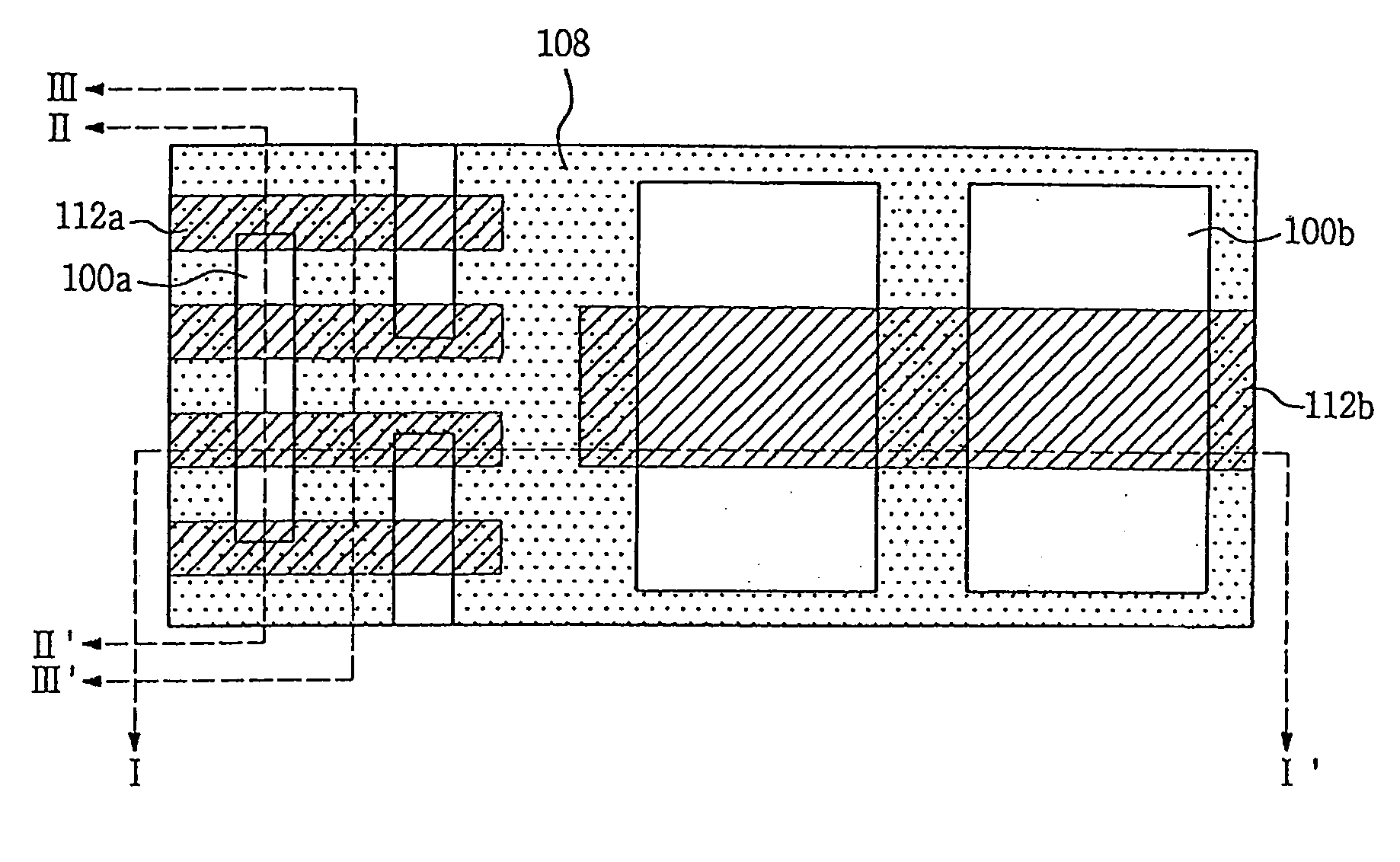
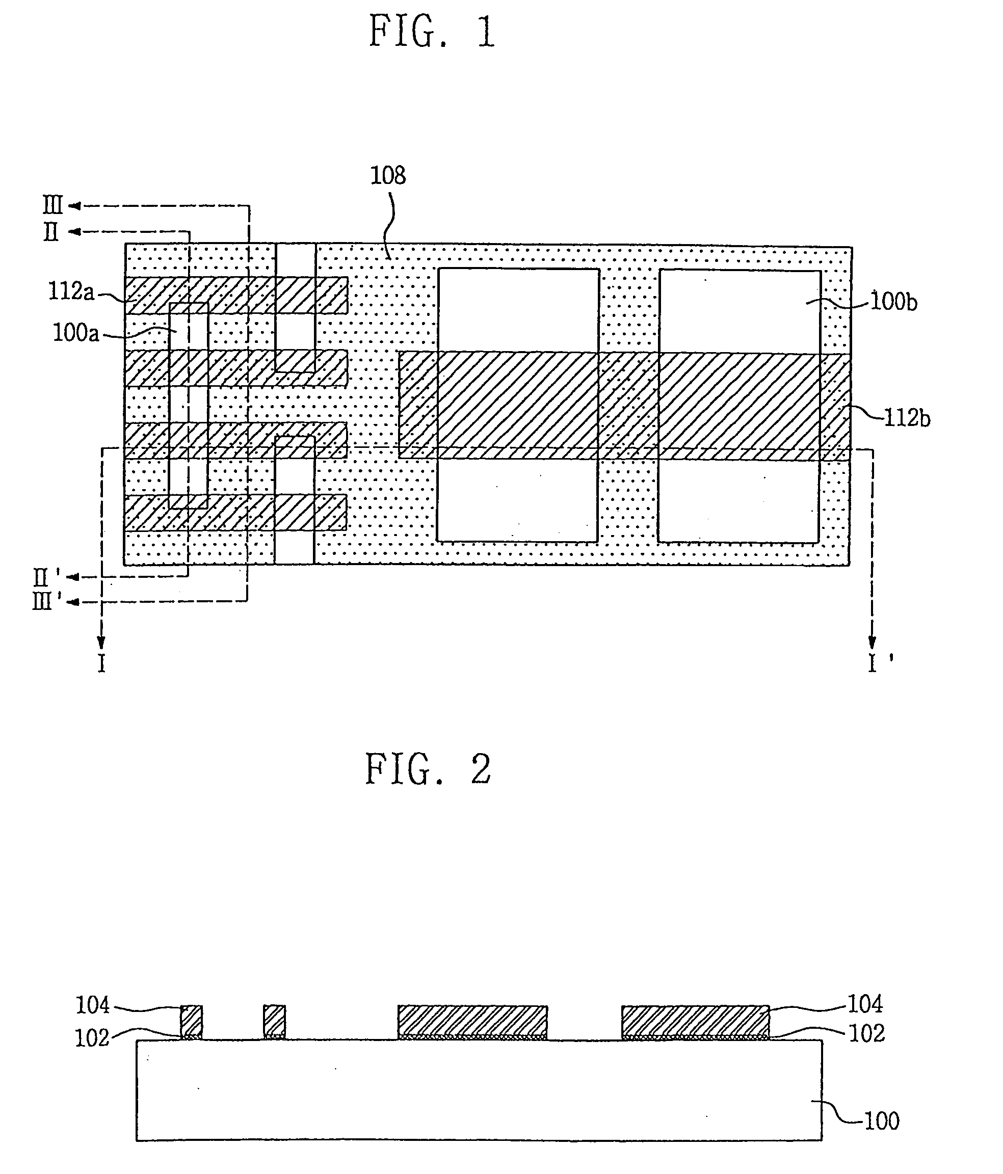
[0021]FIG. 1 is a plan diagram illustrating a finFET according to some embodiments of the invention, and illustrates an active region formed in cell area and peripheral area and a gate electrode.

[0022] Referring to FIG. 1, gate electrodes 112a disposed on active regions 110a are found in a cell area, and a gate electrode 112b disposed on active regions 100b are found in a peripheral area. The active regions 100a and the gate electrodes 112a in the cell area are positioned on the left of the drawing with a relatively small size, and the active regions 100...


PUM


Abstract

According to some embodiments, a fin type active region is formed under an exposure state of sidewalls on a semiconductor substrate. A gate insulation layer is formed on an upper part of the active region and on the sidewalls, and a device isolation film surrounds the active region to an upper height of the active region. The sidewalls are partially exposed by an opening part formed on the device isolation film. The opening part is filled with a conductive layer that partially covers the upper part of the active region, forming a gate electrode. Source and drain regions are on a portion of the active region where the gate electrode is not. The gate electrode may be easily separated and problems causable by etch by-product can be substantially reduced, and a leakage current of channel region and an electric field concentration onto an edge portion can be prevented.

Description

CROSS REFERENCE TO RELATED APPLICATIONS [0001] This application claims priority from Korean Patent Application No. 2003-91716, filed on Dec. 16, 2003, the content of which is hereby incorporated by reference for all purposes. BACKGROUND OF THE INVENTION [0002] 1. Field of the Invention [0003] This disclosure relates to a method of forming a semiconductor device, and more particularly, to a method of forming a fin field effect transistor (finFET) by using a damascene method. [0004] 2. Description of the Related Art [0005] Metal-oxide-semiconductor field effect transistor (MOSFET) is gradually miniaturized for high performance and high integration. To enhance the integration degree of device a new technique has been proposed continuously and this brings about a production of prominent devices from the viewpoint of operation or size. [0006] As one technique to enhance the integration degree of device, a fin field effect transistor was proposed. Such a transistor is formed by a vertical...

Claims


Application Information

Patent Timeline
Patent Type & Authority Applications(United States)
IPC IPC(8): H01L21/336H01L21/84H01L27/12H01L29/786
CPCH01L21/84H01L27/1203H01L29/78609H01L29/785H01L29/7854H01L29/66795H01L21/18
Inventor YOON, JAE-MANJIN, GYO-YOUNGKANG, HEE-SOOPARK, DONG-GUN
Owner SAMSUNG ELECTRONICS CO LTD
Why Eureka
Try Eureka