Method and apparatus for inspecting defects

a technology of defects and inspection methods, applied in the direction of material analysis using wave/particle radiation, semiconductor/solid-state device testing/measurement, instruments, etc., can solve the problem of enormous achieve the effect of reducing binding hours of users for setting test conditions, high sensitivity, and easy and surely

Inactive Publication Date: 2005-08-04
HITACHI LTD
View PDF7 Cites 16 Cited by
  • Summary
  • Abstract
  • Description
  • Claims
  • Application Information

AI Technical Summary

Benefits of technology

[0010] In order to solve the foregoing problems, an object of the present invention is to provide a method and an apparatus for inspecting defects, capable of reducing binding hours for a user, selecting an optimal test condition, and always achieving highly sensitive defect inspection.
[0011] Another object of the present invention is to provide a method and an apparatus for inspecting defects, capable of reducing sensitivity errors between defect inspecting apparatus.
[0028] The present invention is advantageous in that binding hours of a user for setting test conditions can be reduced, even an unskilled user can easily and surely select an optimal test condition, and defect inspection with high sensitivity can always be achieved without any individual differences.

Problems solved by technology

Consequently, a rule of thumb or skills are necessary, and individual differences occur in setting results.
Since setting of the test conditions and the visual verification are repeated, binding hours for test condition setting become enormous for the user.

Method used


Image

  • Method and apparatus for inspecting defects
  • Method and apparatus for inspecting defects
  • Method and apparatus for inspecting defects

Examples


Embodiment Construction

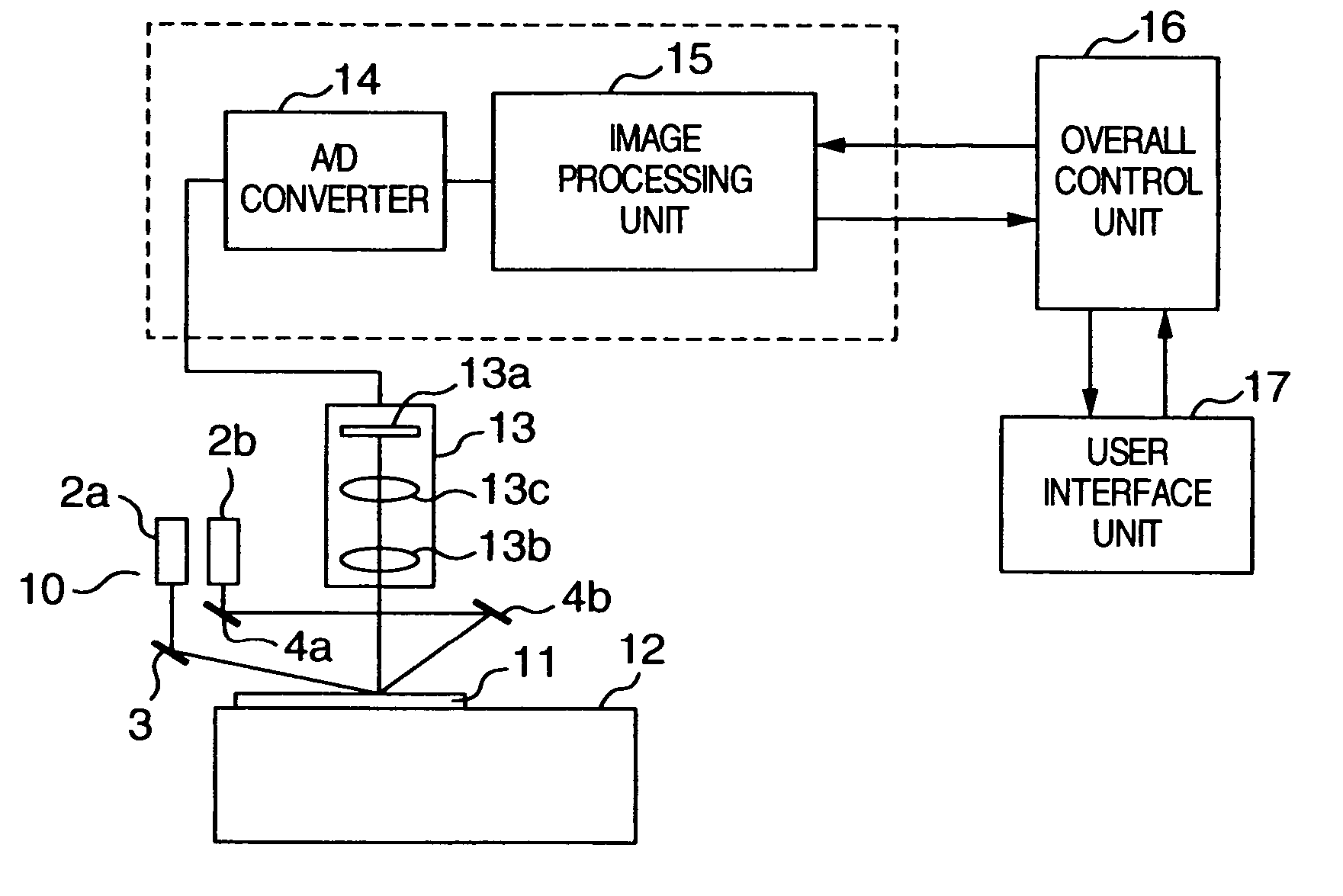
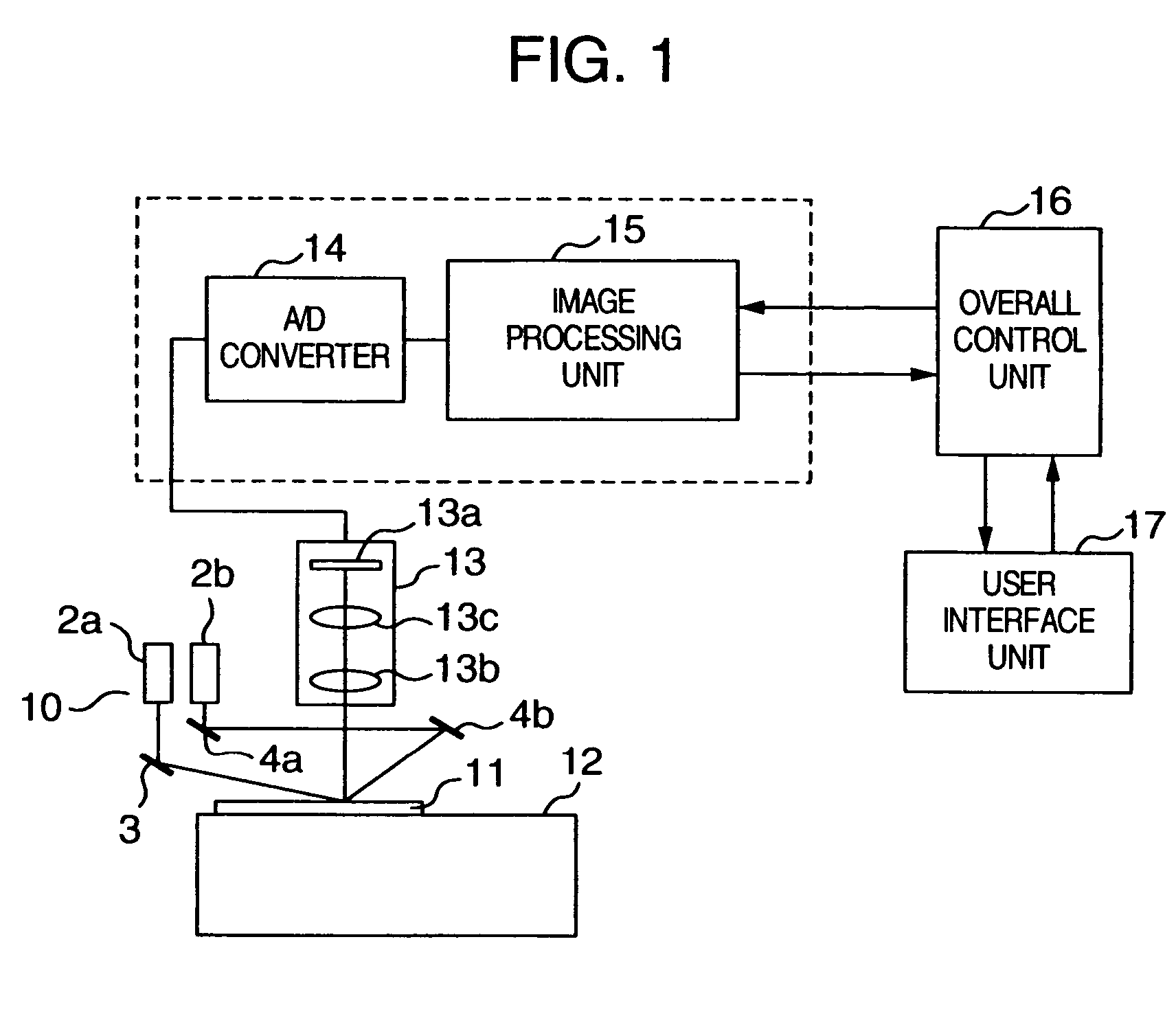
[0043] Next, description will be made in detail for the embodiments of a defect inspecting apparatus according to the present invention with reference to FIGS. 1 to 12.

[0044]FIG. 1 shows a configuration of a bright field optical inspection apparatus as an embodiment of a defect inspecting apparatus according to the invention, where a semiconductor wafer is a target for inspection. The bright field optical inspection apparatus includes: a stage 12 for fixing and moving a semiconductor wafer 11 to be inspected; an illumination optical system 10 for illuminating the semiconductor wafer 11 with UV light or DUV light in a very shallow oblique direction (low angular direction) or a substantially vertical direction (high angular direction) without any physical passage through an objective lens; a detection optical system 13 composed of an objective lens 13b for converging an optical image from the semiconductor wafer 11 illuminated by the illumination optical system 10, an imaging lens 13...


PUM

PropertyMeasurementUnit
angleaaaaaaaaaa
optical inspectionaaaaaaaaaa
wavelength rangeaaaaaaaaaa

Abstract

In a defect inspecting apparatus, having contrast, brightness and appearance of a target for inspection and detection sensitivity of a defect changed depending on optical system conditions, and adapted to perform inspection by selecting an optimal test condition, even an unskilled user can easily select an optimal optical condition by quantitatively displaying evaluation values side by side when optical system conditions are changed. Moreover, by selecting an evaluation item having highest satisfaction based on a result of a series of test inspection, an optimal test condition can be automatically selected.

Description

BACKGROUND OF THE INVENTION [0001] The present invention relates to a method and an apparatus for inspecting defects, capable of inspecting defects such as foreign objects, shape failures and scratches on a substrate to be inspected, e.g., a semiconductor wafer, with high sensitivity by using light or a charged particle beam. [0002] In a defect inspecting apparatus, optical inspection and SEM inspection both include pluralities of conditions: a deflection condition, a wavelength region and the like for the former, and an acceleration voltage, a beam current, the number of scanning times and the like for the latter. Depending on combinations thereof, the number of settable conditions even reaches several tens. One among these conditions is selected to provide highest inspection sensitivity, and then inspection is carried out. [0003] As the conventional art regarding a method of setting optical or charged particle conditions in the defect inspecting apparatus, technologies described i...

Claims


Application Information

Patent Timeline
Patent Type & Authority Applications(United States)
IPC IPC(8): G01B21/30G01B11/30G01N21/94G01N21/95G01N21/956G01N23/04G01N23/06G01N23/225G01N23/227G06T1/00H01L21/66
CPCG01N21/94G01N23/227G01N21/9501
Inventor SAKAI, KAORUMAEDA, SHUNJIOKABE, TAKAFUMIWATANABE, MASAHIRO
Owner HITACHI LTD
Why Eureka
Try Eureka