Semiconductor device and electronic apparatus

a technology of semiconductor devices and electronic devices, applied in the direction of logic circuits using specific components, instruments, unauthorized memory use protection, etc., can solve the problem that the internal algorithm written into the programmable circuit might not be reliably hidden

Inactive Publication Date: 2005-09-08
SHARP KK
View PDF21 Cites 15 Cited by
  • Summary
  • Abstract
  • Description
  • Claims
  • Application Information

AI Technical Summary

Benefits of technology

[0009] The present invention has been attained to solve the above problem, and an object of the present invention is to provide a semiconductor device and an electronic apparatus both of which can hide processing of a circuit in a black-box manner so as to make analysis of an internal algorithm difficult.

Problems solved by technology

However, the conventional semiconductor devices have the problem that an internal algorithm written into the programmable circuit might not be reliably hidden.

Method used


Image

  • Semiconductor device and electronic apparatus
  • Semiconductor device and electronic apparatus
  • Semiconductor device and electronic apparatus

Examples


Embodiment Construction

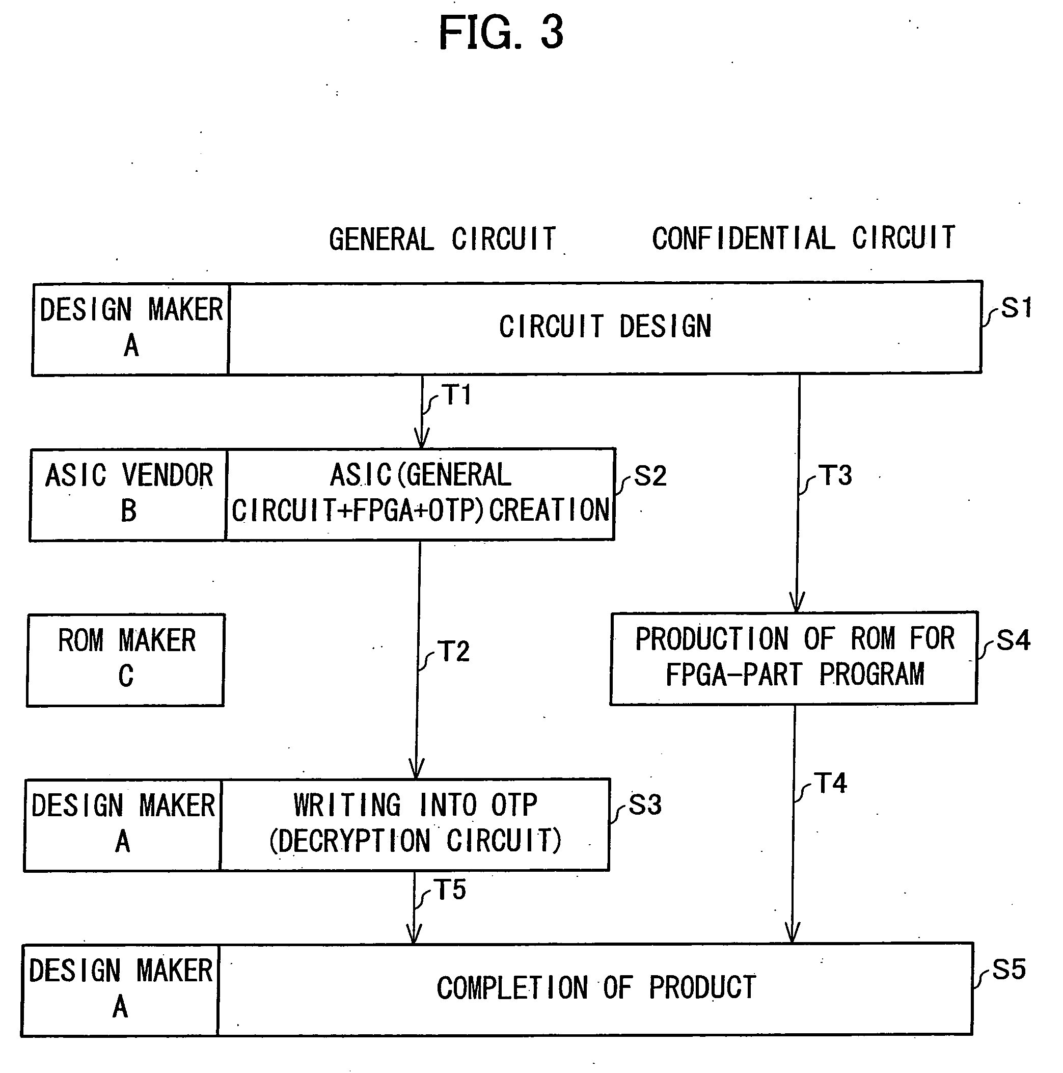
[0029] The following will describe one embodiment of the present invention with reference to FIGS. 1 through 10.

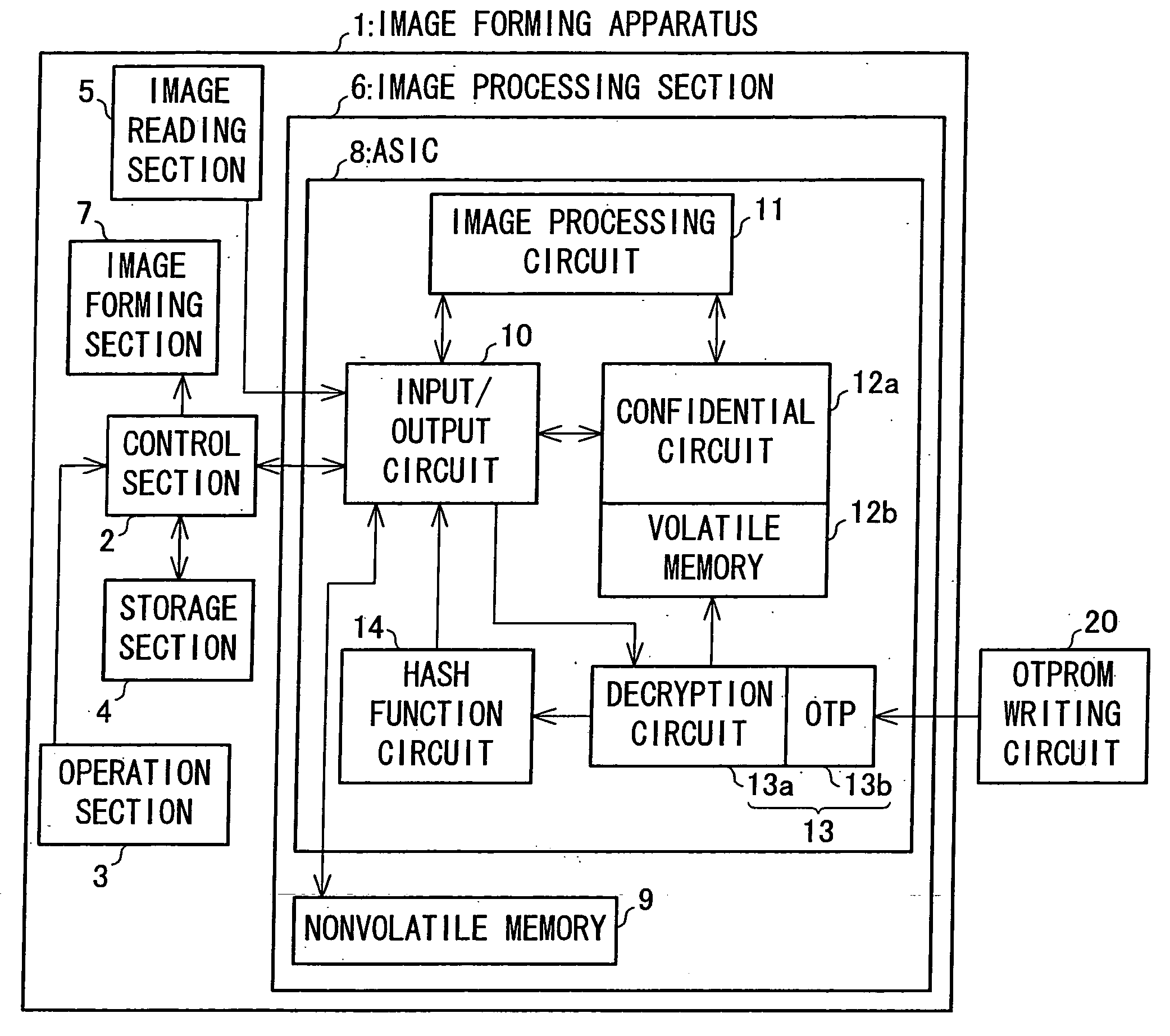
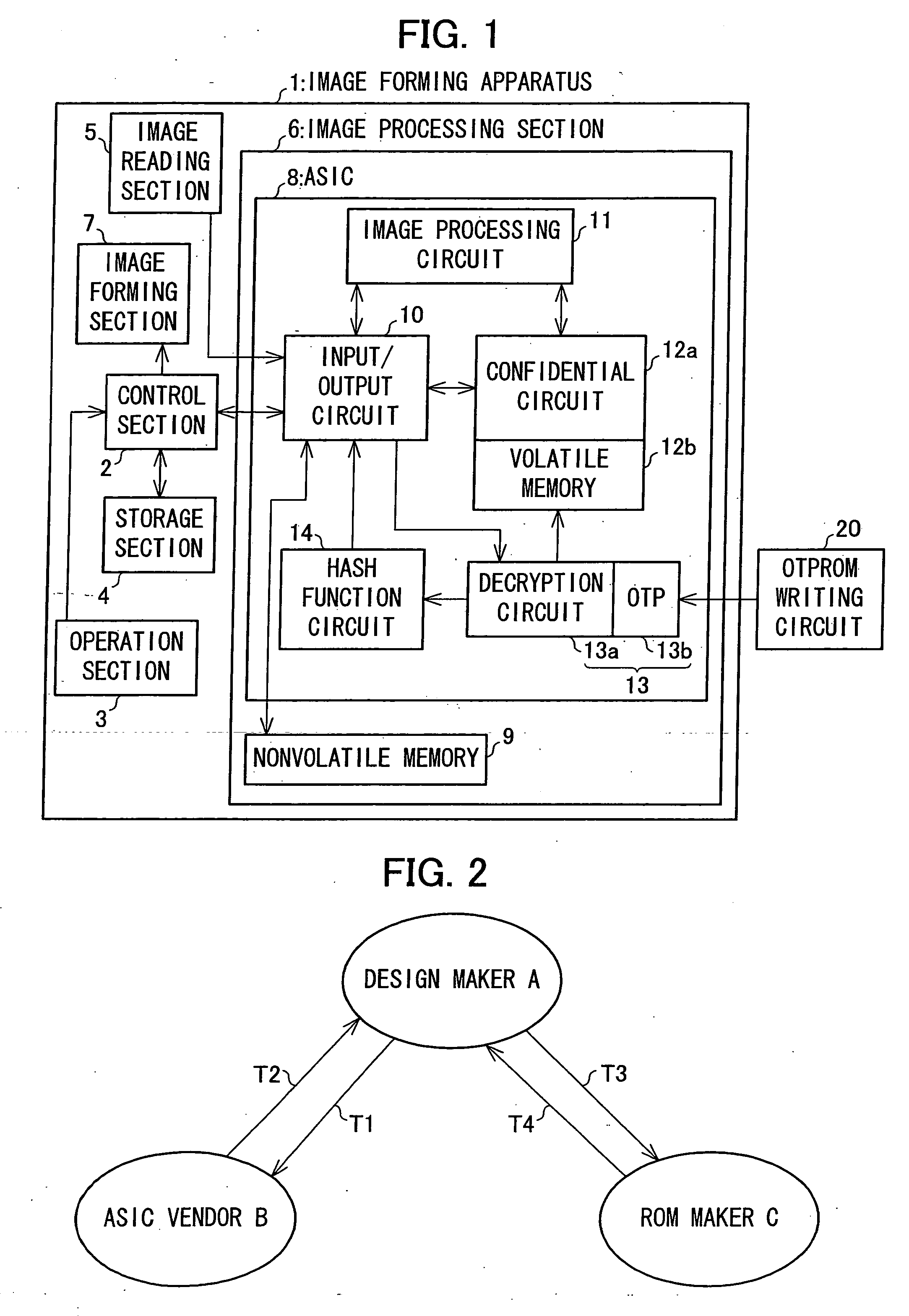
[0030] A semiconductor device of the present embodiment, as illustrated in FIG. 1, is included as an ASIC (Application Specific Integrated Circuit) 8 in an image forming apparatus (electronic apparatus) 1.

[0031] The image forming apparatus 1 forms an image on a sheet. The image forming apparatus 1 can communicate information with an entity outside the image forming apparatus 1 via an input / output interface (not shown).

[0032] The image forming apparatus 1 includes a control section 2, an operation section 3, a storage section 4, an image reading section 5, an image processing section (semiconductor device) 6, and an image forming section 7.

[0033] The control section 2 controls operation of the image forming apparatus 1. The control section 2 of the present embodiment is realized by hardware. However, the present invention is not limited to this. The control section 2 ma...


PUM


Abstract

An ASIC (semiconductor device) of an image processing section is provided with an input/output circuit for performing input and output to and from an image processing circuit and a confidential circuit. The input/output circuit performs output to outside of the ASIC at a timing shifted from a timing of output from the confidential circuit, for example, so as to hide the processing of the confidential circuit. With this arrangement, it is possible to hide an algorithm in the confidential circuit. Further, the ASIC is provided with a decryption circuit for decrypting an encrypted program stored in a nonvolatile memory provided separately from the ASIC. The decryption circuit is caused to function as a decryption section upon later-writing into an OTP.

Description

[0001] This Nonprovisional application claims priority under 35 U.S.C. § 119(a) on Patent Application No. 2004 / 62981 filed in Japan on Mar. 5, 2004, the entire contents of which are hereby incorporated by reference. FIELD OF THE INVENTION [0002] The present invention relates to a semiconductor device including a programmable circuit and an electronic apparatus including the semiconductor device. BACKGROUND OF THE INVENTION [0003] In recent years, attention has been given to programmable circuits that the user can program as desired at his / her site. [0004] For example, an arrangement has been suggested in which part of gate arrays is changed to a FPGA (Field Programmable Gate Array) so that the user can change the processing, holding high speed performance and high packaging density of a masked GA (Gate Array) (see Patent Document 1: Japanese Laid-Open Patent Application No. 1994 / 275718 (Tokukaihei 6-275718; published on Sep. 30, 1994)). [0005] As one example of the use of such a pro...

Claims


Application Information

Patent Timeline
Patent Type & Authority Applications(United States)
IPC IPC(8): G06F21/62G06F3/00G06F12/14G06F21/14G06F21/75G06F21/76G06F21/86H01L21/82H01L27/00H03K19/173H04L9/10
CPCG06F12/1408G06F21/76H04L9/002H04L2209/30H04L9/3263H04L2209/04H04L2209/12H04L9/321
Inventor KAWAKAMI, TAKAHIROKAMEI, NAOYUKIYOSHIMURA, SOHICHIYAMANEKI, KAZUSHI
Owner SHARP KK
Why Eureka
Try Eureka