Maximizing capacitance per unit area while minimizing signal transmission delay in PCB

a signal transmission delay technology, applied in the direction of printed capacitor incorporation, coupling device connection, printed circuit non-printed electric component association, etc., can solve the problems of long delay, common problem of crosstalk, detrimental to the high frequency performance of the connector, etc., to minimize signal transmission delay and maximize compensating capacitance per unit area

Inactive Publication Date: 2005-09-15
COMMSCOPE INC
View PDF38 Cites 19 Cited by
  • Summary
  • Abstract
  • Description
  • Claims
  • Application Information

AI Technical Summary

Benefits of technology

[0009] The present invention overcomes the problems and limitations of the related art crosstalk compensation devices. Particularly, the present invention provides a crosstalk compensating PCB having some layer(s) made of a high dielectric constant (DK) material and other layers made of a low DK material. Then the crosstalk compensating capacitors are made to reside at those layers with the high DK material, while other electronic components are made to reside at the layers with the low DK material. This provides the PCB that maximizes the compensating capacitance per unit area while minimizing signal transmission delays.

Problems solved by technology

Crosstalk is a common problem in devices using connectors.
However, the use of a high DK material for the PCB results in long delays in the signal transmission paths of the conductors between the compensation stages which is detrimental to the high frequency performance of the connector.

Method used


Image

  • Maximizing capacitance per unit area while minimizing signal transmission delay in PCB
  • Maximizing capacitance per unit area while minimizing signal transmission delay in PCB
  • Maximizing capacitance per unit area while minimizing signal transmission delay in PCB

Examples


first embodiment

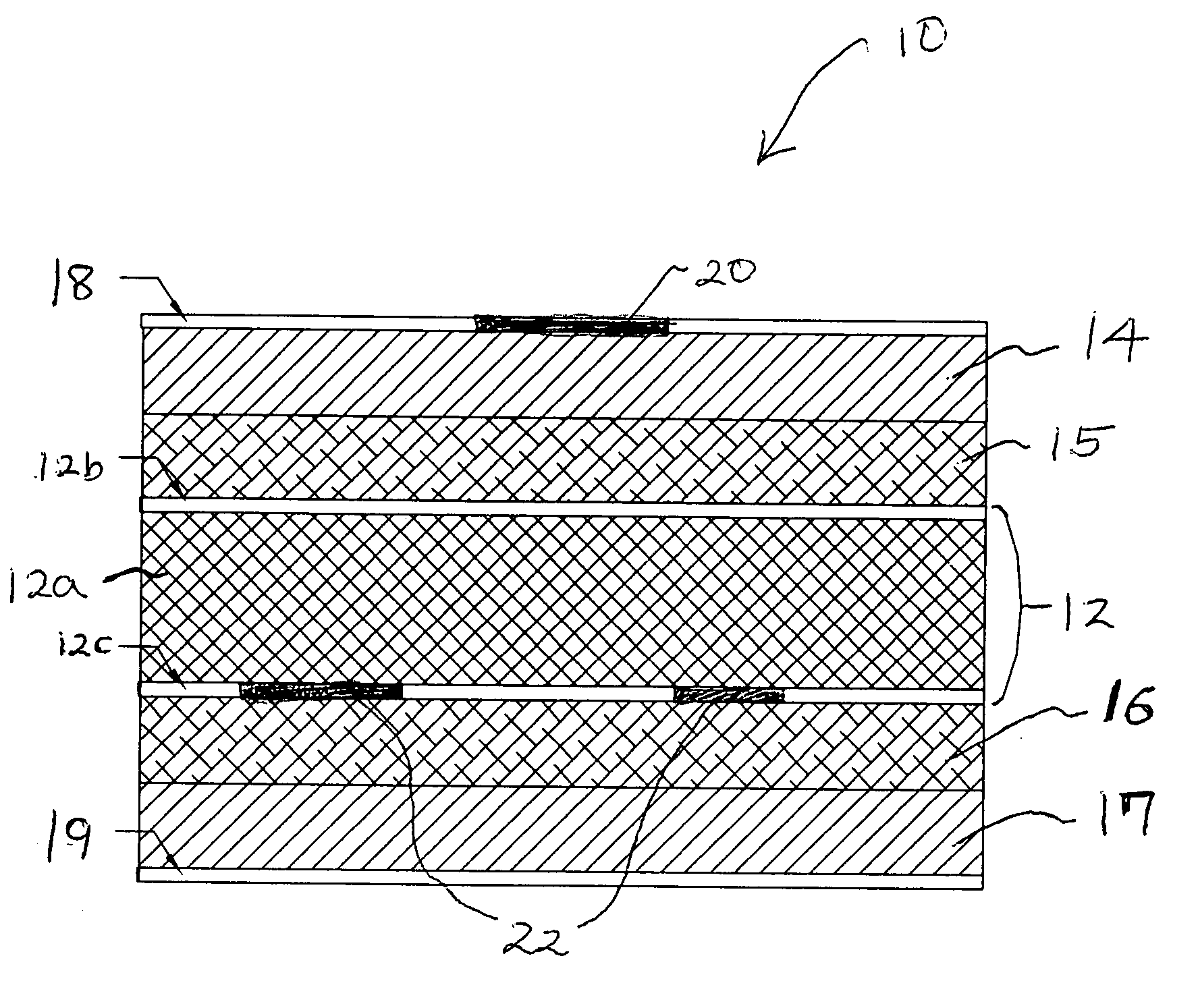
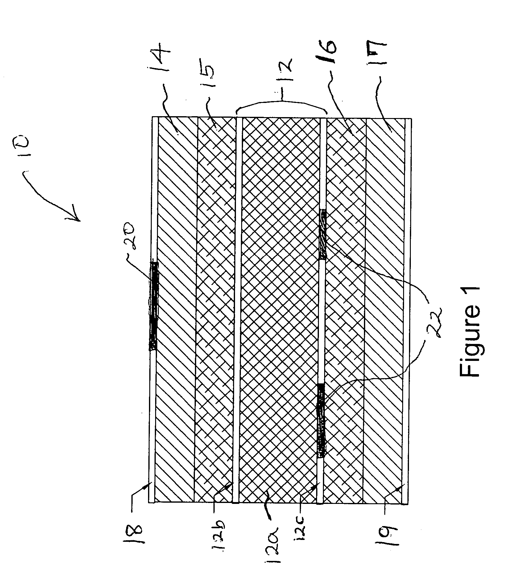
[0016]FIG. 1 is a cross-sectional view of a crosstalk compensating PCB 10 according to the present invention.

[0017] Referring to FIG. 1, the PCB 10 includes a laminate or core 12, first through fourth prepregs 14, 15, 16 and 17, and a plurality of metalized layers 18 and 19. Prepregs are dielectric material sheets known in the art. A laminate / core is also known, and can be made of a copper clad dielectric material substrate 12a with copper sheets (metalized layers) 12b and 12c formed respectively on top and bottom of the dielectric material substrate 12a. The metalized layers 18 and 19 can be a copper foil or other suitable conductive layer.

[0018] The top metalized layer 18, the first prepreg 14 and the second prepreg 15 are stacked up in that order on the top copper sheet 12b of the laminate / core 12. The third prepreg 16, the fourth prepreg 17, and the bottom metalized layer 19 are provided in that order under the bottom copper sheet 12c of the laminate / core 12.

[0019] The laminat...

third embodiment

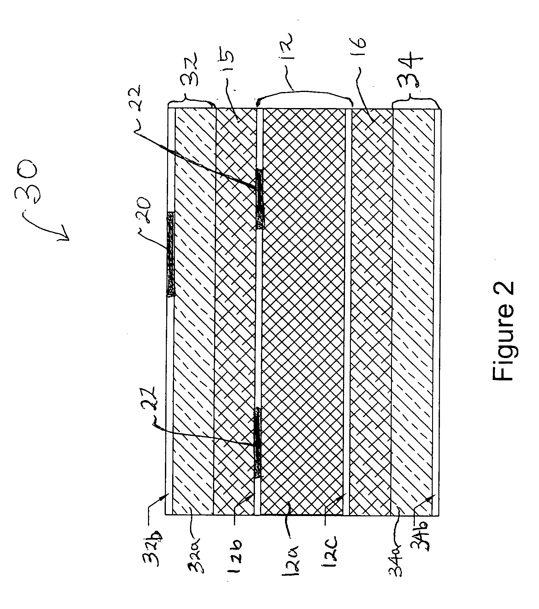
[0028]FIG. 3 is a cross-sectional view of a crosstalk compensating PCB 50 according to the present invention. This embodiment is used when it is desired to have the compensation elements reside on the top and / or bottom metalized layers and the signal transmission paths reside on the inner metalized layers of the PCB 50. In this embodiment, instead of having low DK materials at the outer layers of the PCB and having high DK materials at the inner layers of the PCB as in FIG. 1, low DK materials are present at the inner layers of the PCB and high DK materials are present at the outer layers of the PCB.

[0029] Particularly, referring to FIG. 3, the PCB 50 includes a laminate / core 50, first through fourth prepregs 54, 55, 56 and 57, and the top and bottom metalized layers 18 and 19, all stacked up as shown in FIG. 3. The laminate / core 50 is composed of a low DK substrate 50a (e.g., a low DK copper clad material substrate) and copper sheets 50b and 50c (metalized layers) formed respective...


PUM


Abstract

A printed circuit board (PCB) is provided that maximizes compensation capacitance per unit area of the PCB while minimizing signal transmission delays in the PCB. The PCB includes a first section having a first dielectric constant (DK), a second section having a second DK lower than the first DK and provided above or below the first section, a plurality of crosstalk compensation elements provided in the first section, and a plurality of circuit elements provided in the second section.

Description

BACKGROUND OF THE INVENTION [0001] 1. Field of the Invention [0002] The present invention relates to the field of crosstalk compensation in connectors and, more particularly, to a technique of maximizing capacitance per unit area while minimizing signal transmission delays in crosstalk compensating printed circuit boards (PCBs). [0003] 2. Discussion of the Related Art [0004] Noise or signal interference between conductors in a connector is known as crosstalk. Crosstalk is a common problem in devices using connectors. Particularly, in a system where a modular plug often used with a computer is to mate with a modular jack, the electrical wires (conductors) within the jack and / or plug produce crosstalk. [0005] U.S. Pat. No. 5,997,358 issued to Adriaenssens et al. (hereinafter “the '358 patent”) describes a multi-stage scheme for compensating crosstalk in connectors. The entire contents of the '358 patent are incorporated by reference. Further, the subject matters of U.S. Pat. Nos. 5,91...

Claims


Application Information

Patent Timeline
Patent Type & Authority Applications(United States)
IPC IPC(8): H01R12/04H01R24/00H05K1/02H05K1/11H05K1/16H05K3/46
CPCH05K1/0228H05K1/162H05K3/4626H05K2201/09672H05K2201/09236H05K2201/09536H05K3/4688
Inventor HASHIM, AMIDJOSEPH, ABNER
Owner COMMSCOPE INC
Why Eureka
Try Eureka