Semiconductor component with internal heating

a technology of semi-conductor components and heating chambers, which is applied in the direction of heat measurement, semiconductor/solid-state device testing/measurement, instruments, etc., can solve the problems of non-homogeneous temperature distribution of semi-conductor components in heating chambers, corresponding semi-conductor components may be irreparably damaged and/or destroyed, and more of the semi-conductor components in the heating chamber may be heated too strongly

Inactive Publication Date: 2005-10-06
POLARIS INNOVATIONS
View PDF8 Cites 28 Cited by
  • Summary
  • Abstract
  • Description
  • Claims
  • Application Information

AI Technical Summary

Benefits of technology

[0018] Advantageously, the device for heating the semi-conductor component—pr...

Problems solved by technology

The problem that occurs is that relatively strong non-homogeneous temperature distributions may occur in sections of the heating chamber.
This may lead thereto that one or more of the semi-conductor components in the heating chamber is heated too strongly (for instance above and/or far above the specified temperature in each case, or the target temperature), i.e. is “over-tested”.
Thereby the corresponding semi-conductor component may be irreparably damaged and/or destroyed.
When an attempt is made to avoid the above “over-testing”—i.e. the excessive overheating—of those semi-cond...

Method used


Image

  • Semiconductor component with internal heating
  • Semiconductor component with internal heating
  • Semiconductor component with internal heating

Examples


Embodiment Construction

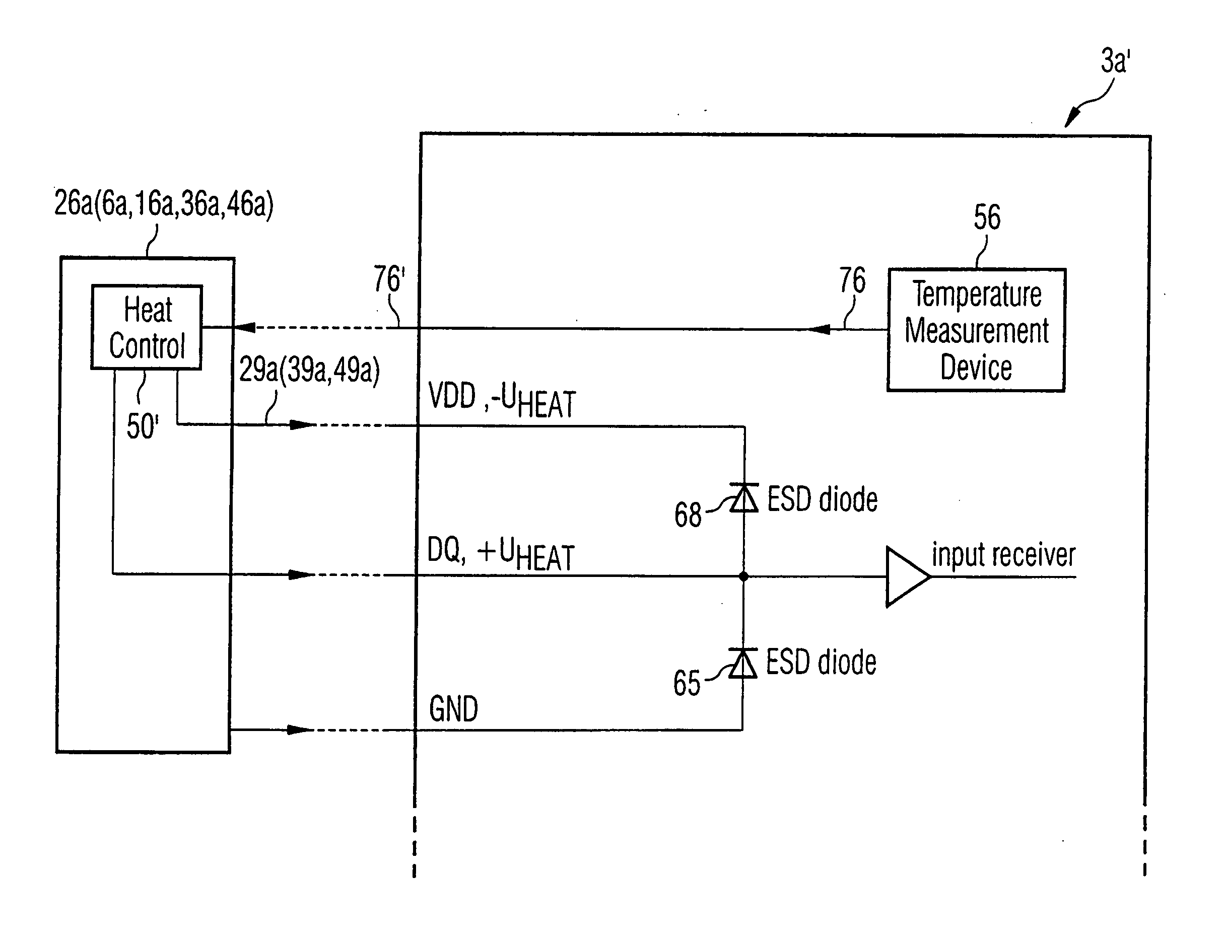
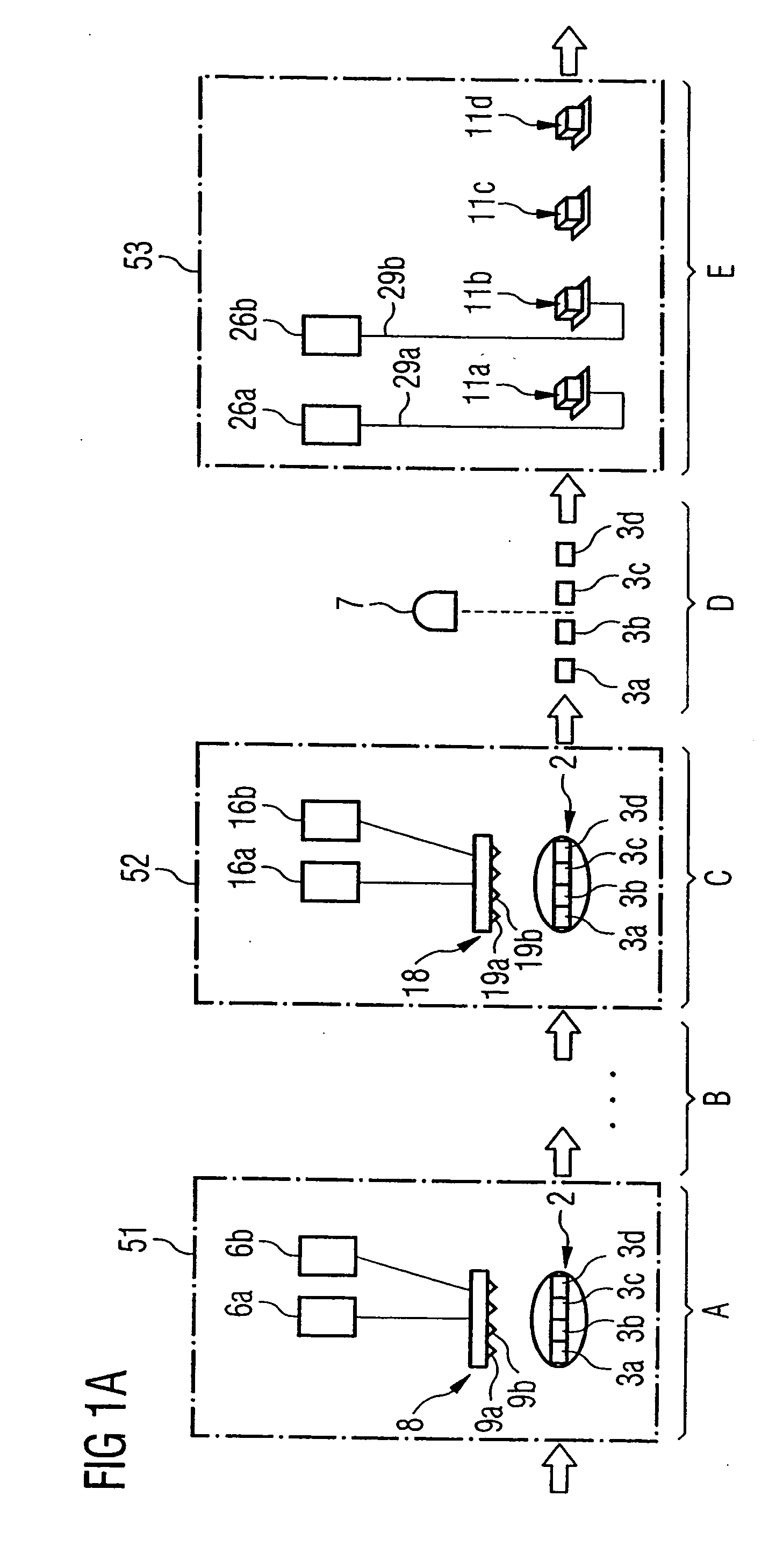
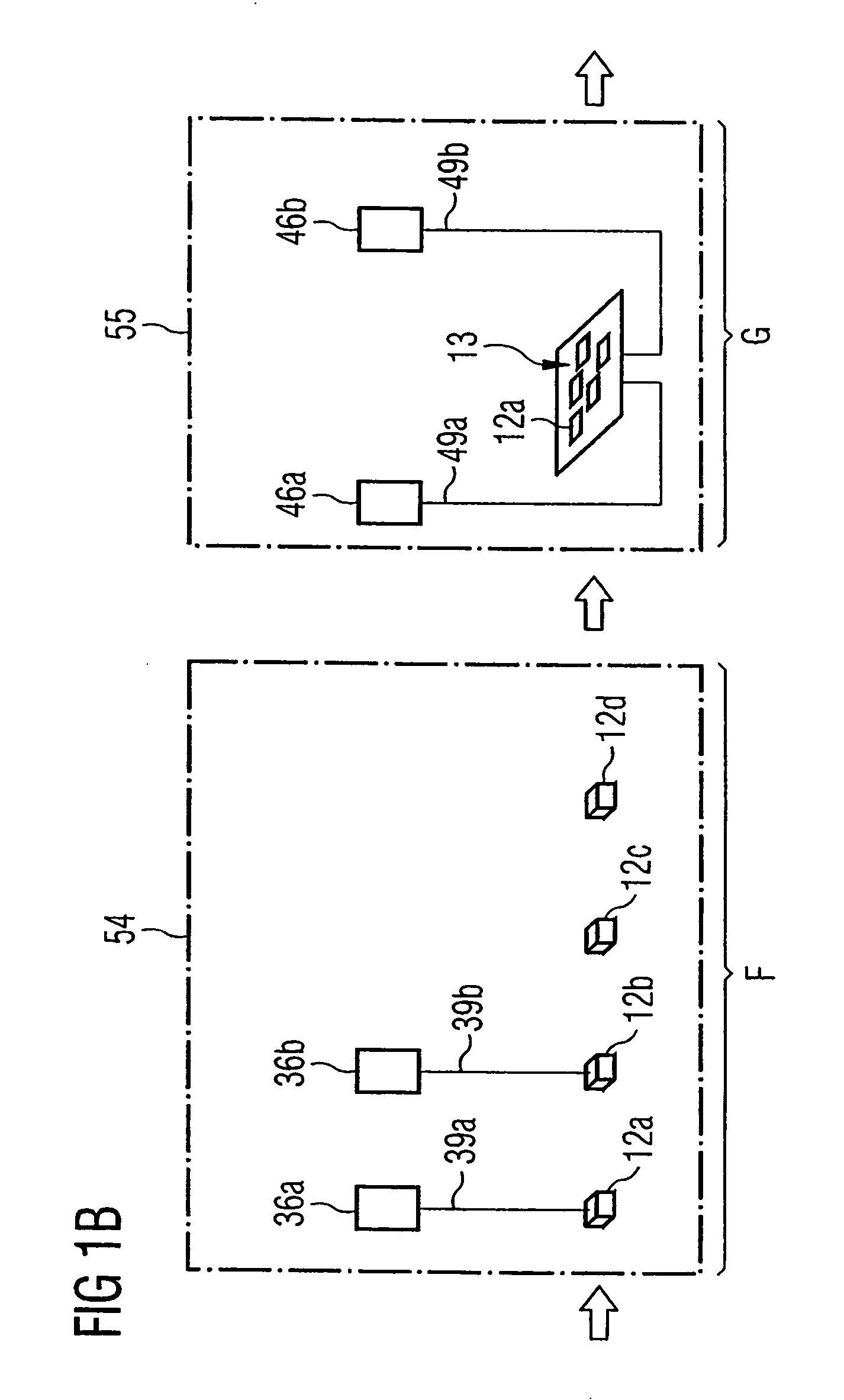
[0026] In FIGS. 1a and 1b, a few stations (some of numerous further stations A, B, C, D, E, F, G not shown here) passed through during the manufacture of semi-conductor components 3a, 3b, 3c, 3d (and / or electronic modules) by the corresponding semi-conductor components 3a, 3b, 3c, 3d are shown schematically.

[0027] The semi-conductor components 3a, 3b, 3c, 3d may for instance be corresponding integrated (analog and / or digital) computing circuitry, and / or semi-conductor memory components such as for instance function storage components (PLAs, PALs, etc.) or table storage components (for instance ROMs or RAMs), in particular SRAMs or DRAMs (here for instance DRAMs (Dynamic Random Access Memories and / or dynamic read-write memories) with double data rate (DDR-DRAMs=Double Data Rate DRAMs), preferably high-speed DDR-DRAMs).

[0028] During the manufacture of the semi-conductor components 3a, 3b, 3c, 3d, a suitable silicon disk and / or corresponding wafer 2 is subjected—for instance at stati...


PUM


Abstract

The invention involves a process for heating a semi-conductor component, as well as a semi-conductor component, whereby a device for heating the semi-conductor component is provided on the semi-conductor component.

Description

CLAIM FOR PRIORITY [0001] This application claims priority to German Application No. 10 2004 015 539.9, filed Mar. 30, 2004, which is incorporated herein, in its entirety, by reference. TECHNICAL FIELD OF THE INVENTION [0002] The invention relates to a semiconductor component with internal heating. BACKGROUND OF THE INVENTION [0003] Semi-conductor components, for instance corresponding integrated (analog and / or digital) computing circuitry, semi-conductor memory components such as for instance function storage components (PLAs, PALs, etc.) and table storage components (for instance ROMs or RAMs, in particular SRAMs and DRAMs), etc. are subjected to numerous tests during and after manufacture. [0004] For instance components (semi-complete and still on the wafer) may be, at one or more stations and with the aid of one or more test apparatuses—even before the wafer has been subjected to all required process steps (i.e. even while the semi-conductor components are still in a semi-comple...

Claims


Application Information

Patent Timeline
IPC IPC(8): G01R31/26G01R31/28G11C29/12H01L21/66H01L23/62H01L27/105
CPCG01R31/2856G11C2029/5002G11C29/12G01R31/2874
Inventor HUBER, THOMASMENCK, PEGGYEGGERS, GEORG
Owner POLARIS INNOVATIONS
Why Eureka
Try Eureka