Image display apparatus and method for manufacturing the same
a technology of image display and apparatus, which is applied in the manufacture of electric discharge tubes/lamps, tubes with screens, discharge tubes luminescnet screens, etc., can solve the problems of affecting the performance of electron-emitting devices, the discharge of electrical current changes, and the failure of electron-emitting devices to work
- Summary
- Abstract
- Description
- Claims
- Application Information
AI Technical Summary
Benefits of technology
Problems solved by technology
Method used
Image
Examples
example 1
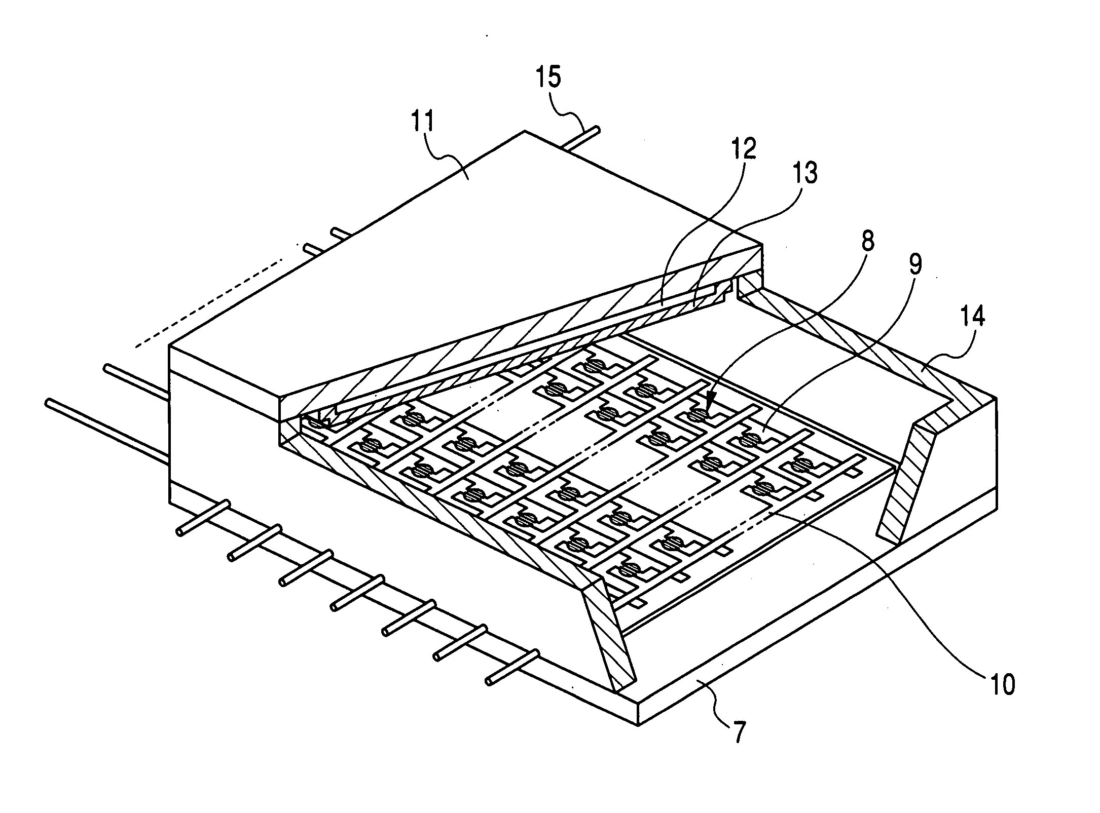
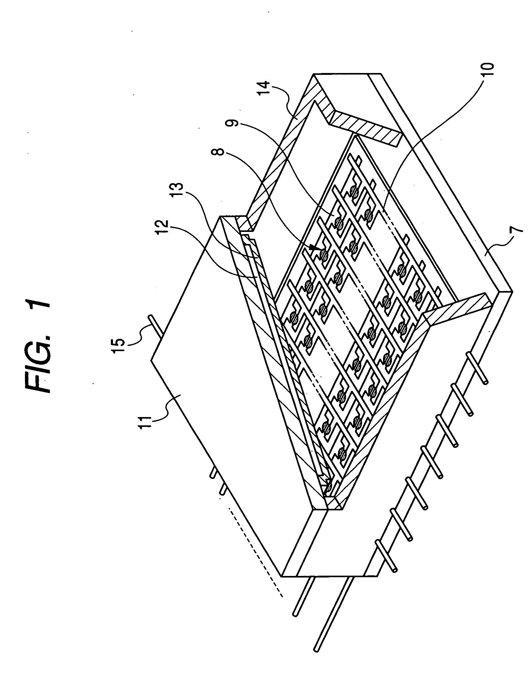
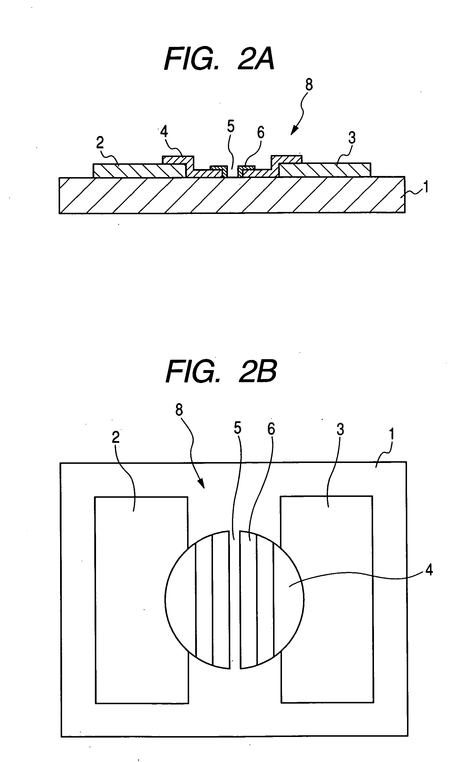
[0066] First, Pt past was printed by an offset printing method on a substrate 1 (in size of 350×300 mm, and in thickness of 5 mm) comprising glass on which an SiO2 layer was formed, and the Pt past was heated to be burned to form the device electrodes 2 and 3 having a thickness of 50 nm on the substrate 1. Moreover, Ag past was printed by the screen printing method, and the Ag paste was heated to be burnt to form the Y-direction wiring 9 (composed of 240 wires) and the X-direction wiring 10 (composed of 720 wires). Insulating paste was printed at the intersection parts of the Y-direction wiring 9 and the X-direction wiring 10 by the screen printing method, and the insulating paste was heated to be burnt to form an insulating layer.
[0067] Next, palladium complex solution was dripped by means of an injection apparatus of a bubble jet (registered trademark) method between the device electrodes 2 and 3. The dripped palladium complex solution was heated at 350° C. for 30 minutes to form...
example 2
[0081] After the deposition of the barium onto the face plate 11 in the Example 1, the getter material of titanium was provided as an adjunct on the barium film to be a thickness of 50 nm by the RF sputtering method. Moreover, only the titanium was provided to be a thickness of 3 nm on the rear plate 7 without forming the barium film. To control the thickness of the titanium material, the deposition rate was suppressed to about 0.1 nm / s to form the titanium film by decreasing RF power and increasing the pressure upon the sputtering. An image display apparatus was produced similarly to the Example 1 except for the respects described above.
[0082] As a result, the discharge current at early stages was twice as much as that of the conventional configuration, and the efficiency was also twice as much as that of the conventional configuration. The characteristics were kept after the elapse of 5000 hours.
example 3
[0083] An image display apparatus was produced similarly to the Example 1 except for using a face plate on which the aluminum metal-back 13 was exposed without deposited barium as the face plate 11, and except for using a rear plate on the whole surface of which aluminum was deposited to be a thickness of 2 nm as the rear plate 7.
[0084] In this case, the deposition of the aluminum having the 2 nm thickness onto the whole surface of the rear plate 7 was performed by an electron beam deposition process in a vacuum container immediately before combining the face plate 11 and the rear plate 7.
[0085] As a result, the electron discharging efficiency at early stages was 1.1%, the discharged current at the early stages was 4.5 microampere, and no changes were generated after the elapse of 5000 hours.
PUM
 Abstract
Description
Claims
Application Information


