Electron emitting devices having metal-based film formed over an electro-conductive film element

a metal-based film and electron-emitting device technology, applied in the manufacture of electric discharge tubes/lamps, tubes with screens, discharge tubes luminescnet screens, etc., can solve the problems of electron-emitting devices not working, electron-emitting devices remarkably deteriorated performance, and change of electric current discharged

Inactive Publication Date: 2007-09-18
CANON KK
View PDF48 Cites 19 Cited by
  • Summary
  • Abstract
  • Description
  • Claims
  • Application Information

AI Technical Summary

Benefits of technology

[0016]It is an objective of the present invention to provide an image display apparatus which can keep the homogeneity of brightness over a long period of time.

Problems solved by technology

However, the conventional image display apparatus disclosed in the Japanese Patent Application Laid-Open No. 2000-251621 has a problem that there appear the changes of electric currents discharged from respective electron-emitting devices when the image display apparatus has performed image displaying over a long period of time of thousands of hours.
In the case where the image forming apparatus is formed by forming the film of the getter material of such a thickness onto the electron-emitting devices on the rear plate, there is produced an evil such that the electron-emitting devices do not work as the electron-emitting devices, or that the performance of the electron-emitting devices is remarkably deteriorated because reactive currents which do not contribute to electron discharging increase.
That is, there is a tendency of the increases in the electric currents of becoming larger in an electron-emitting device which has discharged more electrons.
However, in the image display apparatus, which is ordinarily required to display images changing from moment to moment, the homogeneity of brightness is damaged.
Both of these increases in the electric current and the electron discharging efficiency became the factor which deteriorates the homogeneity of a display image, and they have been serious obstacles for realizing an image display apparatus which is required to perform a high definition image display over a long period of time.

Method used


Image

  • Electron emitting devices having metal-based film formed over an electro-conductive film element
  • Electron emitting devices having metal-based film formed over an electro-conductive film element
  • Electron emitting devices having metal-based film formed over an electro-conductive film element

Examples


example 1

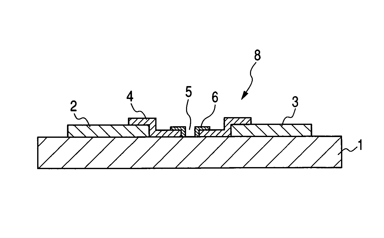
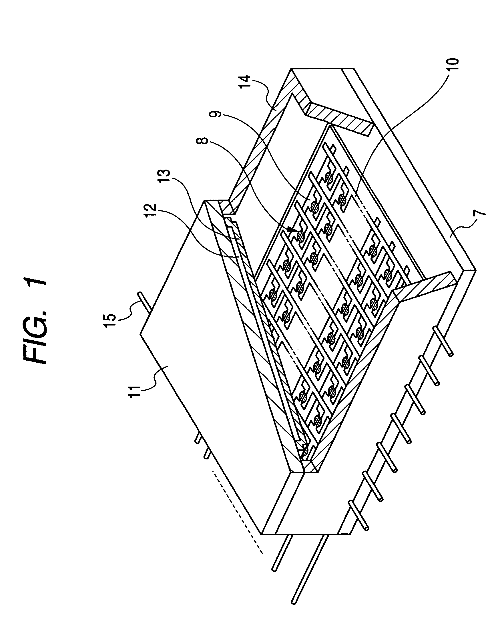
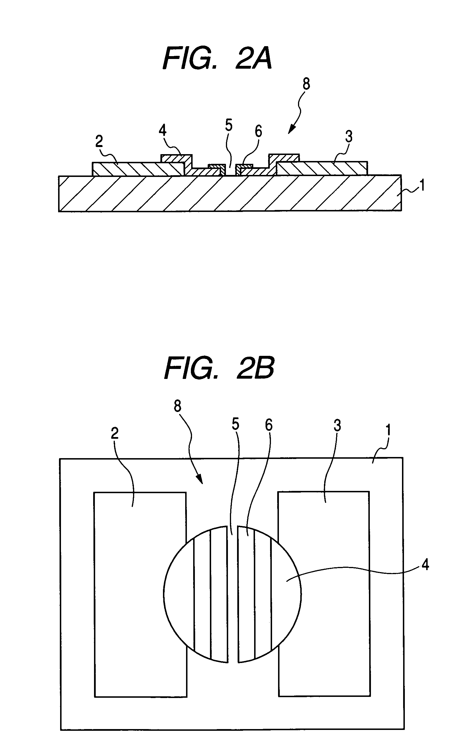
[0066]First, Pt paste was printed by an offset printing method on a substrate 1 (in size of 350×300 mm, and in thickness of 5 mm) comprising glass on which an SiO2 layer was formed, and the Pt paste was heated to be burned to form the device electrodes 2 and 3 having a thickness of 50 nm on the substrate 1. Moreover, Ag paste was printed by the screen printing method, and the Ag paste was heated to be burnt to form the Y-direction wiring 9 (composed of 240 wires) and the X-direction wiring 10 (composed of 720 wires). Insulating paste was printed at the intersection parts of the Y-direction wiring 9 and the X-direction wiring 10 by the screen printing method, and the insulating paste was heated to be burnt to form an insulating layer.

[0067]Next, palladium complex solution was dripped by means of an injection apparatus of a bubble jet (registered trademark) method between the device electrodes 2 and 3. The dripped palladium complex solution was heated at 350° C. for 30 minutes to form...

example 2

[0081]After the deposition of the barium onto the face plate 11 in the Example 1, the getter material of titanium was provided as an adjunct on the barium film to be a thickness of 50 nm by the RF sputtering method. Moreover, only the titanium was provided to be a thickness of 3 nm on the rear plate 7 without forming the barium film. To control the thickness of the titanium material, the deposition rate was suppressed to about 0.1 nm / s to form the titanium film by decreasing RF power and increasing the pressure upon the sputtering. An image display apparatus was produced similarly to the Example 1 except for the respects described above.

[0082]As a result, the discharge current at early stages was twice as much as that of the conventional configuration, and the efficiency was also twice as much as that of the conventional configuration. The characteristics were kept after the elapse of 5000 hours.

example 3

[0083]An image display apparatus was produced similarly to the Example 1 except for using a face plate on which the aluminum metal-back 13 was exposed without deposited barium as the face plate 11, and except for using a rear plate on the whole surface of which aluminum was deposited to be a thickness of 2 nm as the rear plate 7.

[0084]In this case, the deposition of the aluminum having the 2 nm thickness onto the whole surface of the rear plate 7 was performed by an electron beam deposition process in a vacuum container immediately before combining the face plate 11 and the rear plate 7.

[0085]As a result, the electron discharging efficiency at early stages was 1.1%, the discharged current at the early stages was 4.5 microampere, and no changes were generated after the elapse of 5000 hours.


PUM


Abstract

An image display apparatus including a rear plate and a face plate disposed opposite to each other, the rear plate being equipped with a plurality of electron-emitting devices, each provided with a pair of electrodes and an electroconductive film including an electron-emitting region disposed between the electrodes, the face plate being equipped with a phosphor for displaying an image and a film exposed on a surface of the phosphor, the film comprising a metal or a metal compound material. A film comprising the same metal or the same metal compound material as the metal or the metal compound material constituting the film exposed on the surface of the phosphor is formed on each of the electroconductive films of the plurality of electron-emitting devices to have a thickness in a range from 0.2 nm to 4.5 nm.

Description

BACKGROUND OF THE INVENTION[0001]1. Field of the Invention[0002]The present invention relates to an image display apparatus and a method for manufacturing the same. More particularly, the present invention relates to an image display apparatus in which a rear plate equipped with a plurality of electron-emitting devices, and a face plate equipped with a phosphor which displays an image by being irradiated by electrons from the electron-emitting devices are disposed opposite to each other, and a method for manufacturing the same.[0003]2. Related Background Art[0004]There is conventionally known an image display apparatus provided with a rear plate and a face plate which are opposed to each other to be seal-bonded (see, for example, Japanese Patent Application Laid-Open No. 2000-251621). The rear plate is equipped with a plurality of electron-emitting devices in each of which an electroconductive thin film including an electron-emitting region spans a pair of device electrodes. The fac...

Claims


Application Information

Patent Timeline
Patent Type & Authority Patents(United States)
IPC IPC(8): H01J1/30H01J1/304H01J19/24H01J1/316H01J17/49H01J29/28H01J31/12
CPCH01J1/316H01J29/28H01J31/127H01J2201/30426H01J2201/3165B60R16/0215B65D63/1072H02G3/30Y10S174/08
Inventor TAKEDA, TOSHIHIKOYAMAMOTO, KEISUKEKOBAYASHI, TAMAKIMORIGUCHI, TAKUTO
Owner CANON KK
Why Eureka
Try Eureka