
Systems and methods for minimizing static leakage of an integrated circuit

a technology of integrated circuits and static leakage, which is applied in the field of integrated circuits, can solve the problems that the current draw of a device in standby mode referred to as static leakage becomes an increasingly large part of the power budget of the integrated circuit, and achieves the effects of reducing the complexity of the manufacturing process, minimizing static leakage, and minimizing static leakag

Active Publication Date: 2006-01-12
MOSAID TECH
View PDF2 Cites 46 Cited by
  • Summary
  • Abstract
  • Description
  • Claims
  • Application Information

AI Technical Summary

Benefits of technology

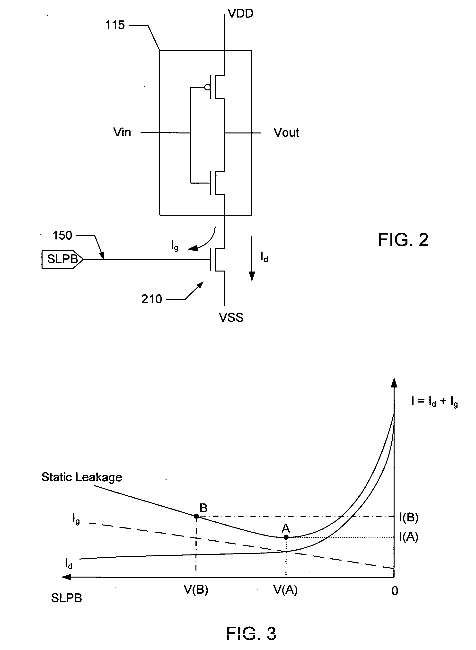
[0011] One advantage of the invention is that because the adaptive leakage controller determines whether to adjust the negative voltage, static leakage is minimized with changes in operating temperature of the integrated circuit, or with voltage fluctuations or manufacturing variations. Rather than a fixed negative voltage, the negative voltage applied to the sleep transistor is adjusted to minimize the static leakage. A further advantage is that single threshold transistor circuitry may be utilized in the integrated circuit, reducing the complexity of the manufacturing process for the integrated circuit. A still further advantage is that the negative voltage may be generated within the integrated circuit, obviating components external to the integrated circuit for generating the negative voltage.
is that because the adaptive leakage controller determines whether to adjust the negative voltage, static leakage is minimized with changes in operating temperature of the integrated circuit, or with voltage fluctuations or manufacturing variations. Rather than a fixed negative voltage, the negative voltage applied to the sleep transistor is adjusted to minimize the static leakage. A further advantage is that single threshold transistor circuitry may be utilized in the integrated circuit, reducing the complexity of the manufacturing process for the integrated circuit. A still further advantage is that the negative voltage may be generated within the integrated circuit, obviating components external to the integrated circuit for generating the negative voltage.

Problems solved by technology

However, as component device size scales from 250 nanometers to 130 nanometers or below, a current draw of a device in standby mode referred to as static leakage becomes an increasingly large part of the power budget of the integrated circuit.

Method used


Image

  • Systems and methods for minimizing static leakage of an integrated circuit
  • Systems and methods for minimizing static leakage of an integrated circuit
  • Systems and methods for minimizing static leakage of an integrated circuit

Examples


Embodiment Construction

[0022] As shown in the exemplary drawings wherein like reference numerals indicate like or corresponding elements among the figures, exemplary embodiments of a system and method according to the present invention are described below in detail. It is to be understood, however, that the present invention may be embodied in various forms. For example, although described herein as pertaining to minimizing static leakage of an integrated circuit, aspects of the invention may be practiced on circuitry not embodied within an integrated circuit. Therefore, specific details disclosed herein are not to be interpreted as limiting, but rather as a basis for the claims and as a representative basis for teaching one skilled in the art to employ the present invention in virtually any appropriately detailed system, structure, method, process or manner.

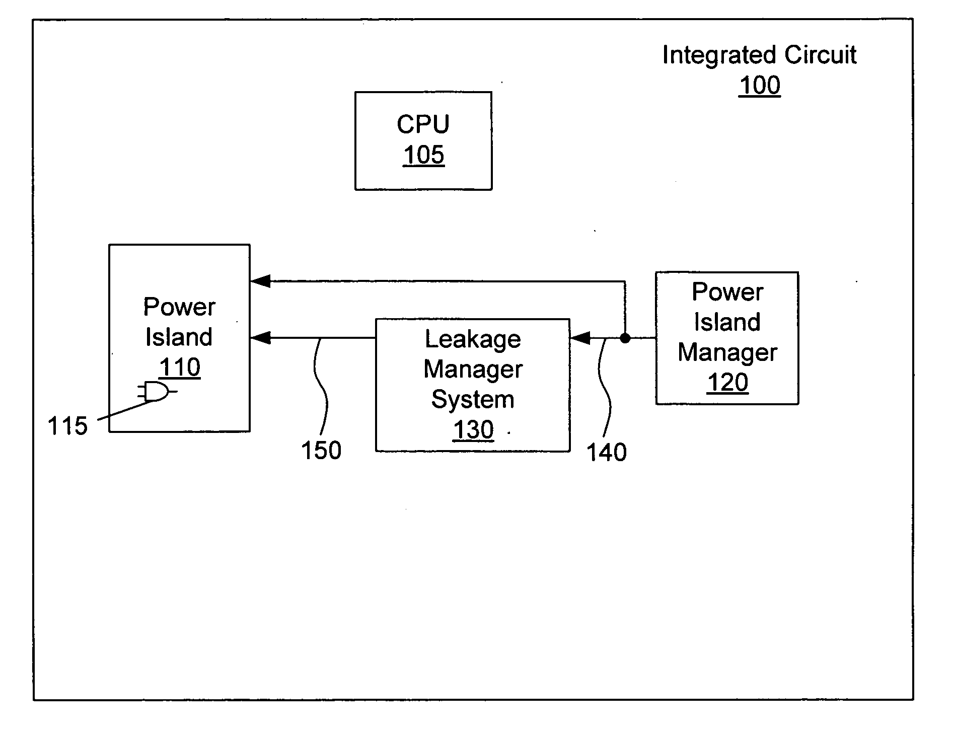
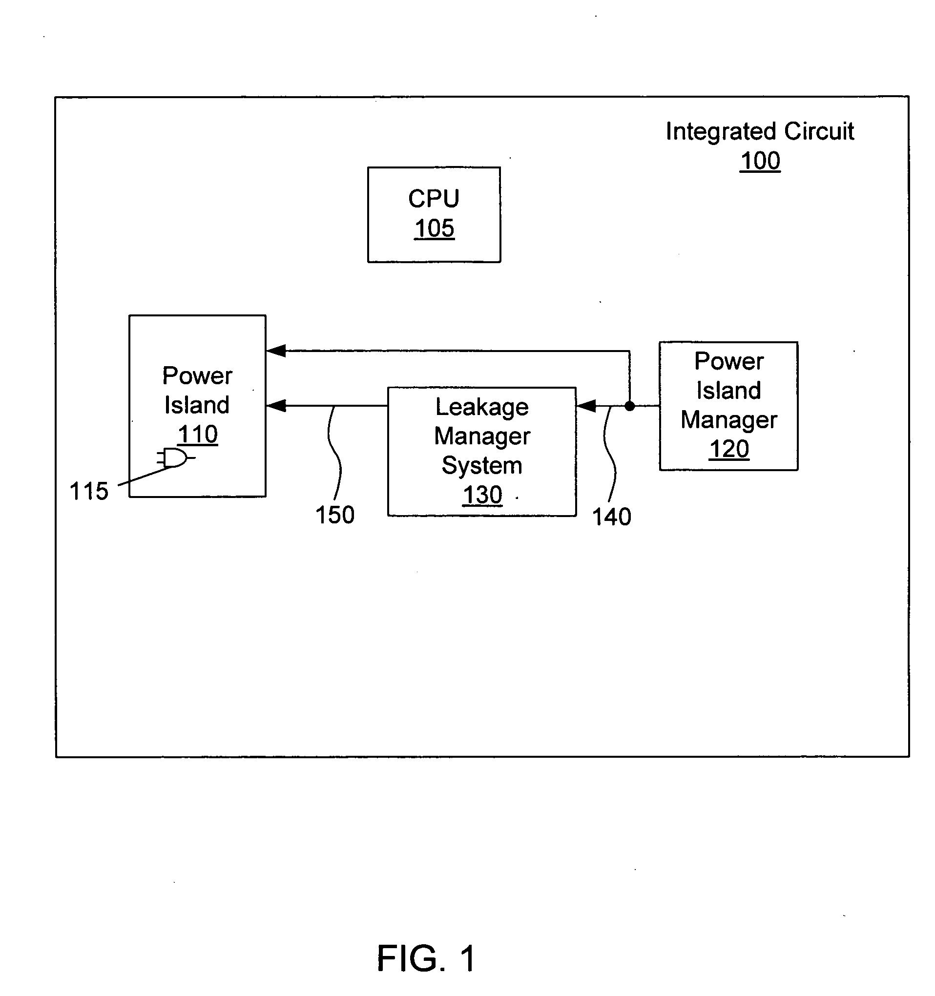
[0023]FIG. 1 is a block diagram of an integrated circuit 100 embodying a system for minimizing static leakage, in accordance with one embodiment of ...


PUM


Abstract

To minimize static leakage of an integrated circuit, a charge pump generates a negative voltage to be applied to a “sleep” transistor cascaded to a logic gate of the integrated circuit. An adaptive leakage controller determines continuously or periodically whether to adjust the negative voltage to minimize the static leakage. A negative voltage regulator adjusts the negative voltage depending on the determination. Some embodiments determine whether to adjust the negative voltage by monitoring one or more parameters of the sleep transistor. Some embodiments determine whether to adjust the negative voltage by monitoring one or more parameters of an emulated sleep transistor.

Description

CROSS-REFERENCE TO RELATED APPLICATIONS [0001] This application claims the benefit of U.S. Provisional Application No. 60 / 586,565 titled “Systems and Methods for I / O and Power Island Management and Leakage Control on Integrated Circuits,” filed Jul. 9, 2004, which is hereby incorporated by reference. This application is also related to U.S. patent application Ser. No. 10 / 840,893, titled “Managing Power on Integrated Circuits Using Power Islands,” filed May 7, 2004, which is hereby incorporated by reference.BACKGROUND [0002] 1. Field of the Invention [0003] The present invention relates generally to integrated circuits, and more particularly to systems and methods for applying a negative voltage in integrated circuits. [0004] 2. Description of the Prior Art [0005] One design goal for integrated circuits is to reduce power consumption. Devices with batteries such as cell phones and laptops particularly need a reduction in power consumption in the integrated circuit to extend the life ...

Claims


Application Information

Patent Timeline
IPC IPC(8): G05F1/10
CPCH03K19/0016G05F1/10
Inventor CAPLAN, RANDY J.SCHWAKE, STEVEN J.
Owner MOSAID TECH
Learn More