Method for controlling ph during planarization and cleaning of microelectronic substrates

a microelectronic substrate and control method technology, applied in the direction of grinding machine components, manufacturing tools, lapping machines, etc., can solve the problems of affecting the subsequent processing steps, affecting the relative motion between the substrate and the polishing pad, and not creating a sufficient planer surface on the substrate.

Inactive Publication Date: 2006-01-19
MICRON TECH INC
View PDF9 Cites 1 Cited by
  • Summary
  • Abstract
  • Description
  • Claims
  • Application Information

AI Technical Summary

Benefits of technology

[0013] The present invention is directed toward methods and apparatuses for processing a microelectronic substrate. In one embodiment, the apparatus can include a polishing pad having a planarizing surface and a source of planarizing liquid in fluid communication with the planarizing surface of the polishing pad. The microelectronic substrate is planarized by engaging the substrate with the polishing pad while the planarizing liquid is disposed on the polishing pad, and moving one of the substrate and the polishing pad relative to the other of the substrate and the polishing pad. As the relative motion between the substrate and the polishing pad is decreased, rinsing fluid having a pH approximately the same as a pH of the planarizing liquid can be introduced to the planarizing surface to maintain the pH of the microelectronic substrate at an approximately constant level.

Problems solved by technology

One drawback with the conventional methods discussed above is that they may not create a sufficiently planer surface on the substrate because particulates may remain attached to the substrate as a result of contact between the substrate 12 and a variety of chemical solutions during and after planarization.
These particulates may damage the wafer during subsequent polishing and handling steps, or may interfere with subsequent processing steps, such as masking and etching.
Furthermore, the particulates may become incorporated into the devices formed on the substrate, potentially causing the devices to fail.
Accordingly, a further drawback with the conventional processes described above is that they may require additional time to remove the particulates from the substrate.

Method used


Image

  • Method for controlling ph during planarization and cleaning of microelectronic substrates
  • Method for controlling ph during planarization and cleaning of microelectronic substrates
  • Method for controlling ph during planarization and cleaning of microelectronic substrates

Examples


Embodiment Construction

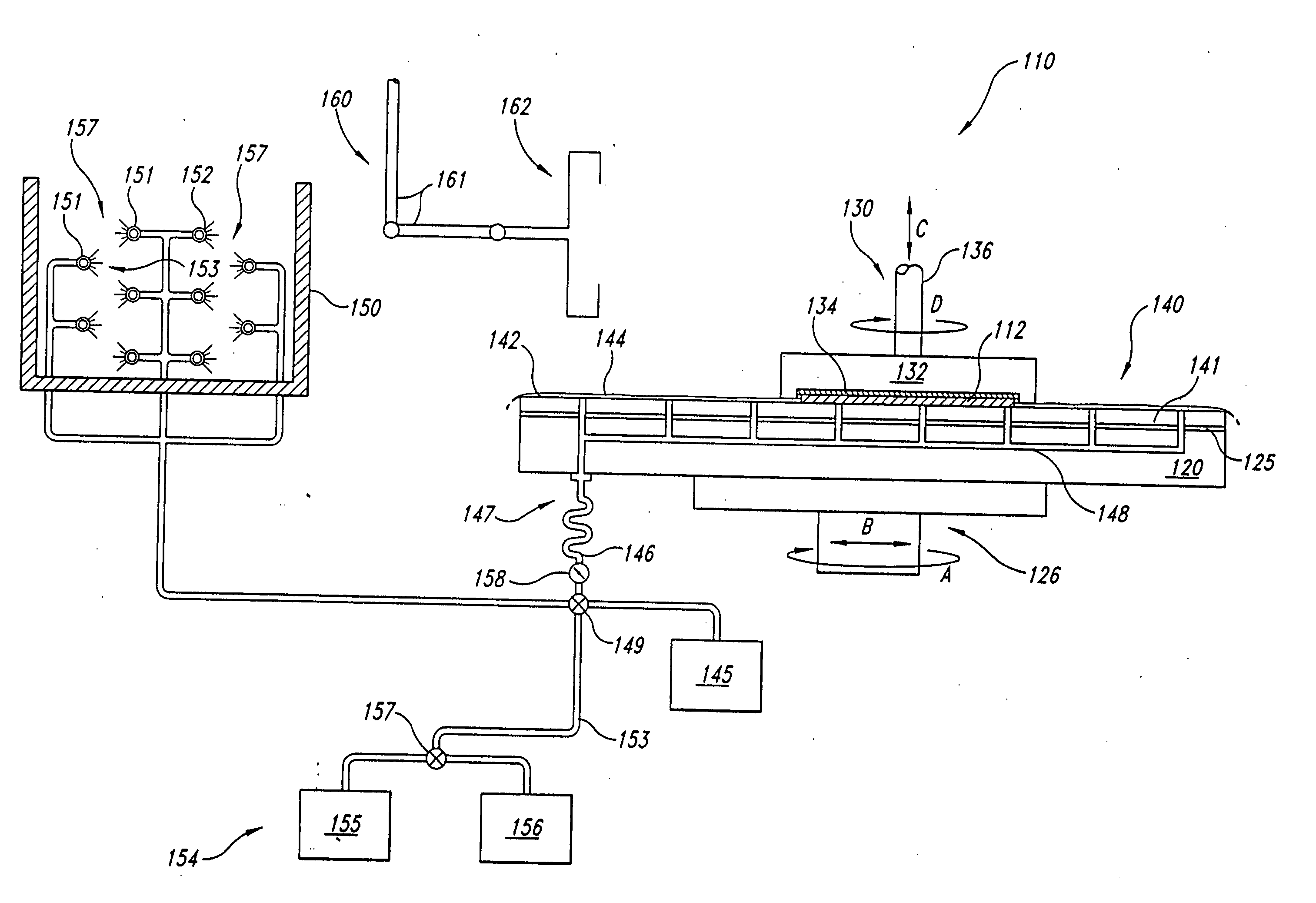
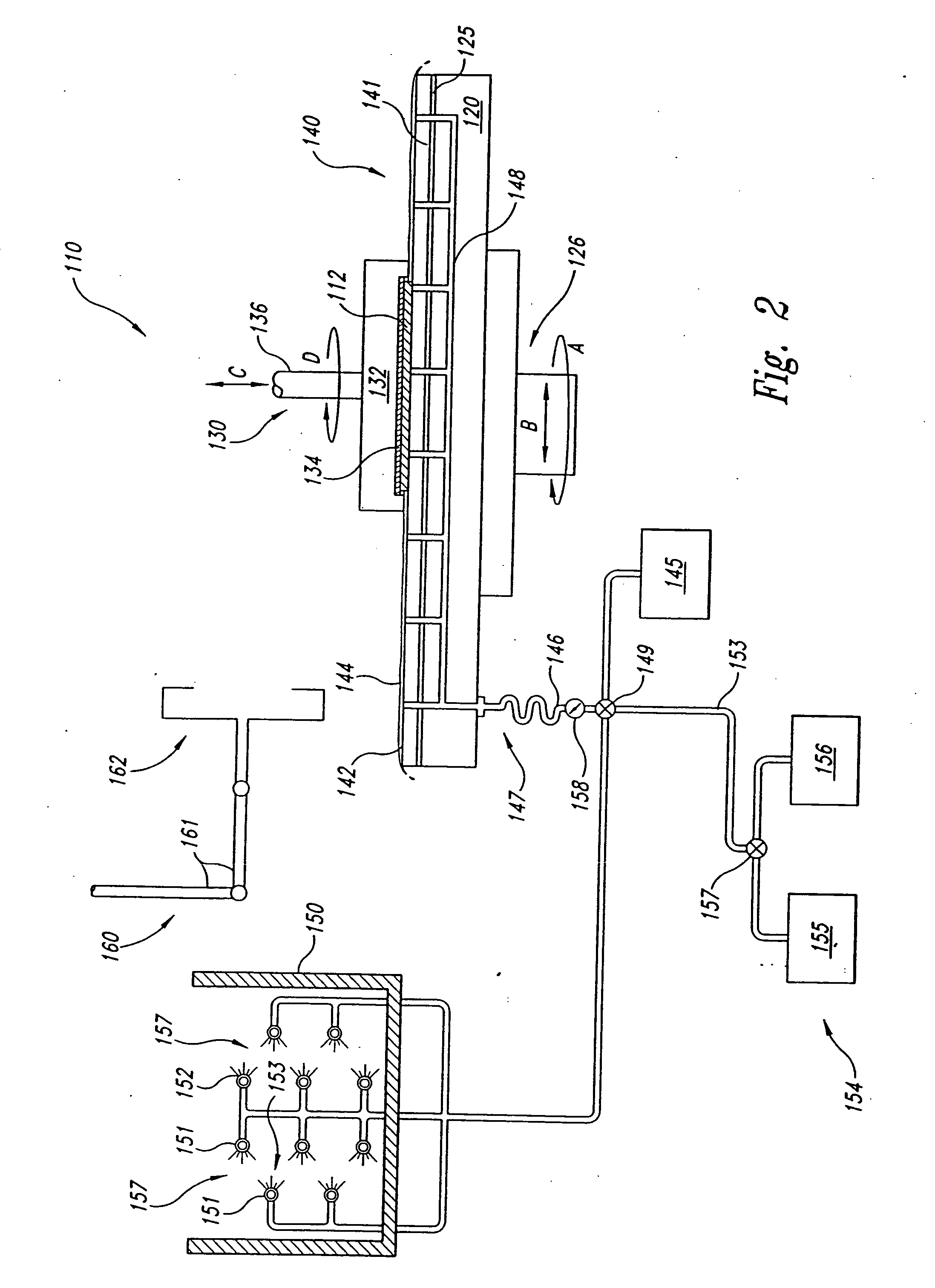
[0020] The present invention is an apparatus and method for mechanical and / or chemical-mechanical planarization of substrates used in the manufacture of microelectronic devices. Many specific details of certain embodiments of the present invention are set forth in the following description and in FIGS. 2-3 to provide a thorough understanding of such embodiments. One skilled in the art, however, will understand that the present invention may have additional embodiments or that the invention may be practiced without several of the details described in the following description.

[0021]FIG. 2 is a schematic side elevation view of a CMP machine 110 having a platen 120 and a planarizing medium 140. In one embodiment, the CMP machine can include a model number 676 manufactured by IPEC Corp. of Portland, Oreg., and in other embodiments, the CMP machine can include other devices, such as a web-format planarizing machine, manufactured by EDC Corporation. In the embodiment shown in FIG. 2, the...


PUM

PropertyMeasurementUnit
timeaaaaaaaaaa
timeaaaaaaaaaa
timeaaaaaaaaaa

Abstract

A method and apparatus for processing a microelectronic substrate. In one embodiment, the method can include planarizing the microelectronic substrate with a planarizing liquid and rinsing the substrate with a rinsing liquid having a pH approximately the same as a pH of the planarizing liquid. The rinsing step can be completed while the substrate remains on a polishing pad of the apparatus, or, alternatively, the substrate can be removed to a rinsing chamber for rinsing. In another embodiment, the method can include conditioning the polishing pad by removing polishing pad material from the polishing pad and then cleaning the microelectronic substrate by engaging the substrate with the same polishing pad and moving at least one of the polishing pad and the substrate relative to the other of the polishing pad and the substrate after conditioning the polishing pad.

Description

TECHNICAL FIELD [0001] The present invention relates to mechanical and chemical-mechanical planarization of microelectronic substrates. More particularly, the present invention relates to controlling the pH of a microelectronic substrate during planarization and post-planarization processing of the microelectronic substrate. BACKGROUND OF THE INVENTION [0002] Mechanical and chemical-mechanical planarization processes remove material from the surfaces of semiconductor wafers, field emission displays, and many other microelectronic substrates to form a flat surface at a desired elevation. FIG. 1 schematically illustrates a planarizing machine 10 with a platen or base 20, a carrier assembly 30, a polishing pad 41 positioned on the platen 20, and a planarizing liquid 44 on the polishing pad 41. The planarizing machine 10 can also have an under-pad 25 attached to an upper surface 22 of the platen 20 for supporting the polishing pad 41. In many planarizing machines, a drive assembly 26 ro...

Claims


Application Information

Patent Timeline
Patent Type & Authority Applications(United States)
IPC IPC(8): C23F1/00H01L21/461B24B37/04B24B49/00B24B57/02H01L21/306
CPCB24B37/0056B24B37/04B24B37/042H01L21/02052B24B57/02H01L21/02024B24B49/00
Inventor SHARPLES, JUDSON R.ZACHARIAS, KENNETH F.HUDSON, GUY F.
Owner MICRON TECH INC
Why Eureka
Try Eureka