
Methods of forming magnetic shielding for a thin-film memory element

a technology of thin-film memory and shielding, which is applied in the direction of digital storage, semiconductor devices, instruments, etc., can solve the problems of limiting the influence of thin-film magnetic memory, adversely affecting the information stored in an adjacent memory cell, and increasing the likelihood, so as to reduce undesirable fields and enhance desirable magnetic fields

Inactive Publication Date: 2006-03-23
MICRON TECH INC
View PDF7 Cites 0 Cited by
  • Summary
  • Abstract
  • Description
  • Claims
  • Application Information

AI Technical Summary

Benefits of technology

[0015] The present invention overcomes many of the disadvantages of the prior art by providing a monolithically formed ferromagnetic thin-film memory that has local shielding on at least two sides of a magnetic bit region. The local shielding helps protect the magnetic bit from externally generated EMI, internally generated cross-talk, and other internally and externally generated noise. In addition, when the local shielding layers are provided adjacent a word line and / or digital line, the local shielding layers may help concentrate the magnetic fields of the word lines and / or digital lines at the magnetic bit regions, in much the same way as a magnetic field keeper. Accordingly, the shielding layers may not only help reduce undesirable fields from influencing the magnetic bit regions, but may also enhance the desirable magnetic fields at the magnetic bit regions.
[0016] In one illustrative embodiment, top and bottom shielding layers are provided above and below a conventional monolithically formed magneto-resistive memory element, although it is contemplated that any type of magnetic memory element may be used. The memory element is preferably formed on the underlayers of a conventional monolithic integrated circuit. This helps provide easy electrical interconnection between the memory cells and the memory operating circuitry on the monolithic integrated circuit. The shielding layers are also preferably monolithically formed.
[0017] In another illustrative embodiment, a word line is provided adjacent the memory elements, with a first shielding layer extending adjacent the word line. A second shielding layer is provided adjacent a digital line, which preferably extends along the other side of the memory elements. To help reduce internally generated cross-talk, the first and / or second shielding layers may extend along the side surfaces of the word line and / or digital line, respectively. As indicated above, this may enhance the desired magnetic fields at the memory element and reduce cross-talk.

Problems solved by technology

Reducing the dimensions of the word lines and digital lines, however, tends to reduce the current that can be accommodated thereby, and thus the magnetic field that can be produced at the corresponding magnetic bit regions.
However, this increases the likelihood that the magnetic field produced by one word line or digital line may adversely affect the information stored in an adjacent memory cell.
In this configuration, the upper and lower shielding layers may help shunt externally generated fields, limiting their influence on the thin-film magnetic memory.
A limitation of using shielded packages is that the shielding layers may not protect the magnetic bits from internally generated fields, such as those produced by adjacent word or digital lines or the like.
A limitation of Pisharody is that only one side of each memory cell has a superconducting magnetic field keeper.

Method used


Image

  • Methods of forming magnetic shielding for a thin-film memory element
  • Methods of forming magnetic shielding for a thin-film memory element
  • Methods of forming magnetic shielding for a thin-film memory element

Examples


Embodiment Construction

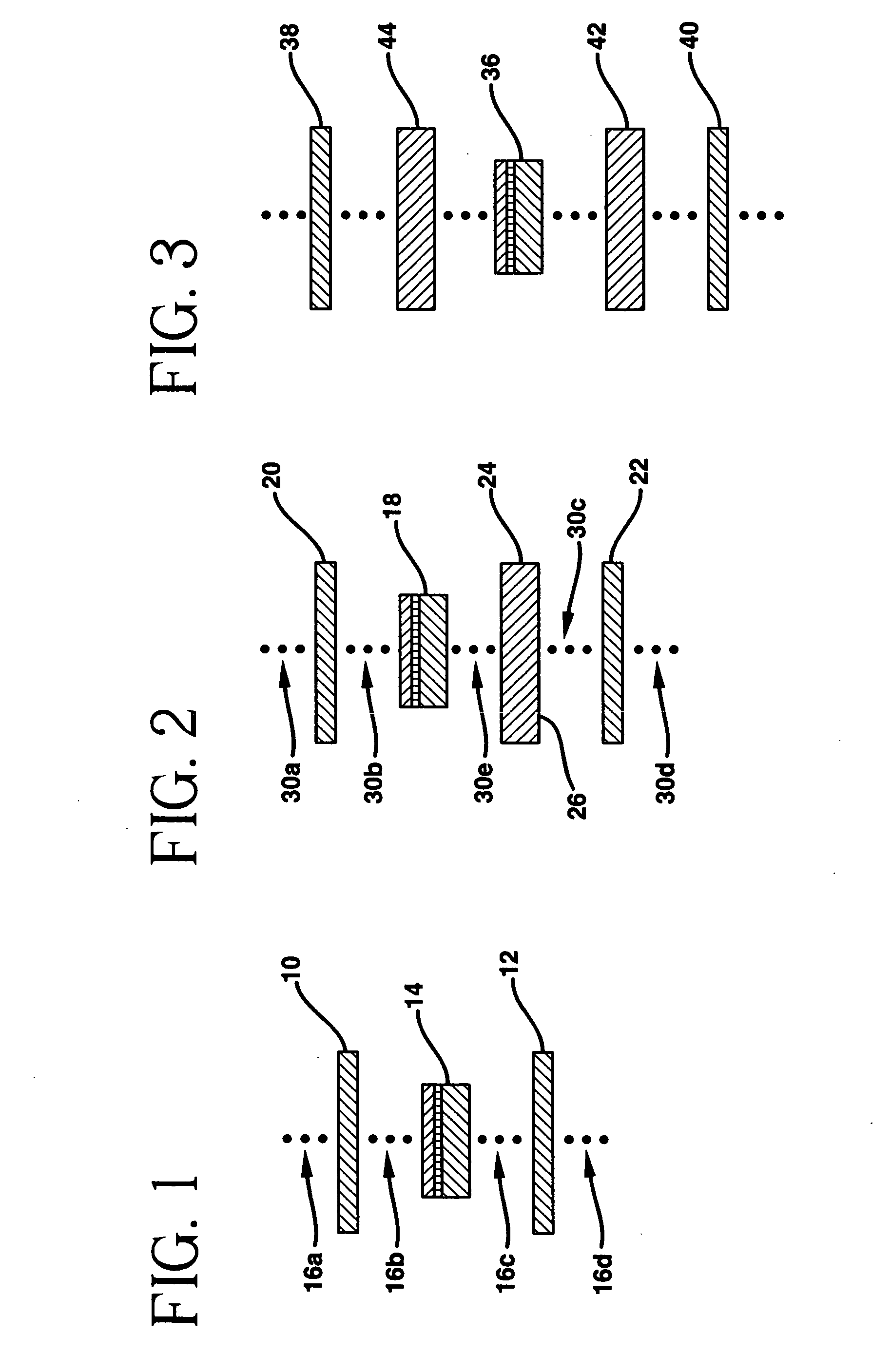
[0043]FIG. 1 is a cross section of a monolithic memory element that has an upper shield and a lower shield. The upper shield 10 is provided above memory element 14, and lower shield 12 is provided below memory element 14. It is contemplated that any type of magnetic memory element 14 may be used.

[0044] The memory element 14 is preferably formed above the underlayers of a conventional integrated circuit. This helps provide easy electrical interconnection between the memory cells and the memory operating circuitry on the monolithic integrated circuit. The shielding elements 10 and 12 are also preferably monolithically formed with the integrated circuit and the memory element 14.

[0045] The dots at 16b and 16c indicate that one or more layers may be interposed between the memory element 14 and the upper and lower shield elements 10 and 12, respectively. In the embodiment shown, all that is important is that at least two sides, such as the upper and lower sides of the memory element 14...


PUM


Abstract

A monolithically formed ferromagnetic thin-film memory is disclosed that has local shielding on at least two sides of selected magnetic storage elements. The local shielding preferably extends along the back and side surfaces of a word line and / or digital lines of a conventional magnetic memory. In this configuration, the local shielding not only may help reduce externally generated EMI, internally generated cross-talk and other unwanted fields in the magnetic bit region, but may also help enhance the desired magnetic fields in the bit region.

Description

RELATED APPLICATION [0001] This application is a divisional of U.S. patent application Ser. No. 09 / 318,073, filed May 25, 1999, titled “Thin Film Memory Device Having Local And External Magnetic Shielding,” the disclosure of which is incorporated by reference herein in its entirety. CROSS REFERENCE TO CO-PENDING APPLICATIONS [0002] The present application is related to U.S. patent application Ser. No. 08 / 993,005 filed Dec. 18, 1997, titled “HIGH DENSITY MAGNETIC MEMORY DEVICE AND METHOD OF MANUFACTURE THEREFOR,” now U.S. Pat. No. 6,048,739, issued on Apr. 11, 2000; and U.S. patent application Ser. No. 08 / 993,009, filed Dec. 18, 1997, titled “Self-Aligned Wordline Keeper and Method of Manufacture Therefor,” now U.S. Pat. No. 5,956,267, issued on Sep. 21, 1999, which are assigned to the assignee of the present application, the disclosures of which are hereby incorporated by reference in their entireties herein.GOVERNMENT RIGHTS [0003] This invention was made with Government support un...

Claims


Application Information

Patent Timeline
Patent Type & Authority Applications(United States)
IPC IPC(8): H01L21/00G11C11/14G11C11/15G11C11/16H01L43/12
CPCG11C11/14H01L43/12G11C11/16G11C11/15G11C11/161H10N50/01H01L27/10
Inventor ZHU, THEODORESATHER, JEFFREY S.
Owner MICRON TECH INC
Learn More