Reducing or eliminating color change for microcavity OLED devices

a technology of organic light and oled, which is applied in the direction of discharge tube/lamp details, discharge tube luminescnet screens, other domestic articles, etc., can solve the problems of inability to reduce the color change, limit the use of resonant oled structures in a number, and the emission spectrum of microcavity devices

Active Publication Date: 2006-03-30
DOLYA HOLDCO 5 LTD
View PDF12 Cites 82 Cited by
  • Summary
  • Abstract
  • Description
  • Claims
  • Application Information

AI Technical Summary

Problems solved by technology

Unfortunately, microcavity devices have an emission spectrum that undesirably varies as a function of viewing angle from the display.
This blue shift limits the use of the resonant OLED structure in a number of important applications,

Method used


Image

  • Reducing or eliminating color change for microcavity OLED devices
  • Reducing or eliminating color change for microcavity OLED devices
  • Reducing or eliminating color change for microcavity OLED devices

Examples


first embodiment

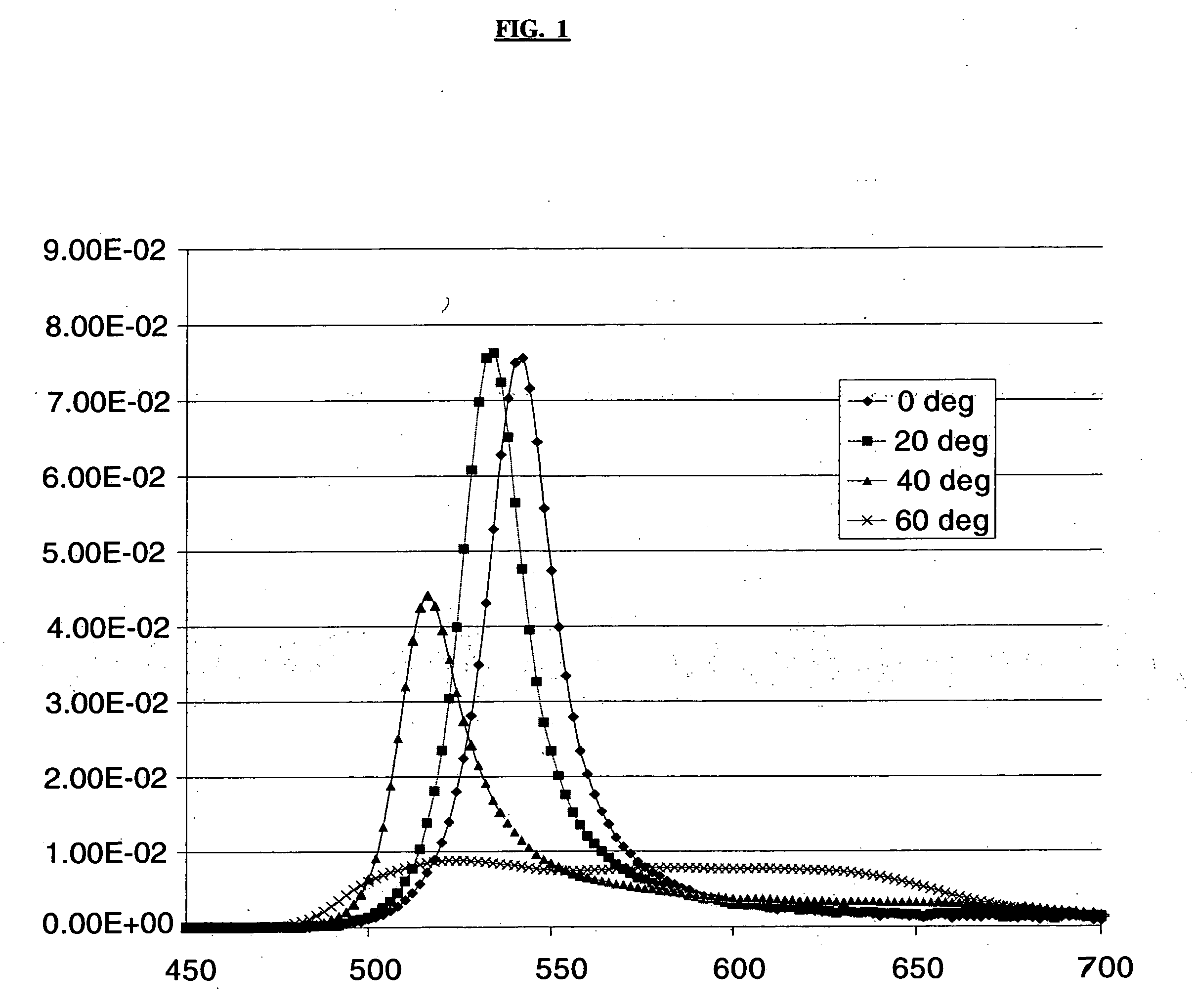
[0051]FIG. 7 graphically shows a prospective example of the resulting emission spectrums when the microstructure is used to reduce or eliminate the color change at different viewing angles. The microstructure refracts wavelengths at angles less than 30° but internally reflects wavelengths at angles greater than 30° and thus the emission spectrums at the viewing angles greater than 30° are eliminated (e.g., the emission spectrum at the 40° viewing angle and the emission spectrum at the 60° viewing angle have been eliminated). Because of the greater blue-shifting occurring at the larger viewing angles (e.g., the 40° and the 60° viewing angles) and thus the greater likelihood that the perceived color will change at these larger angles, the elimination of the emission spectrums at these larger viewing angles greatly reduces the likelihood that there will be a perceived color change at different viewing angles. Because the internally reflected wavelengths are randomly outputted at the al...

second embodiment

[0053]FIG. 8 graphically shows a prospective example of the resulting emission spectrums when the microstructure is used to reduce or eliminate the color change at different viewing angles. The microstructure redistributes the wavelengths so that the outputted emission spectrums are broader and there is no perceived color change at the different viewing angles. The intensity of the wavelengths of the emission spectrums are increased due to the presence of the microstructure. In FIG. 8, the emission spectrum at the 0° viewing angle has a peak emitted wavelength at about 540 nm which is a dark green color. Similarly, the emission spectrum at the 40° viewing angle has a peak emitted wavelength at about 533 nm which is also the dark green color. The intensity is insignificant at the wavelengths of both emission spectrums where there is a different hue (e.g., at a wavelength of about 505 nm, the color is a blue-green color) and so both emission spectrums have the same perceived color whi...


PUM

PropertyMeasurementUnit
Angleaaaaaaaaaa
Coloraaaaaaaaaa
Microstructureaaaaaaaaaa

Abstract

In an embodiment of the invention, a microcavity OLED device that minimizes or eliminates color change at different viewing angles is fabricated. The OLED device can be, for example, an OLED display or an OLED light source used for area illumination. This OLED device includes a multi-layer mirror on a substrate, and each of the layers are comprised of a non-absorbing material. The OLED device also includes a first electrode on the multi-layered first mirror, and the first electrode is substantially transparent. An emissive layer is on the first electrode. A second electrode is on the emissive layer, and the second electrode is substantially reflective and functions as a mirror. The multi-layer mirror and the second electrode form a microcavity. On a front surface of the substrate is a light modulation thin film. The light modulation thin film can be any one of: a cut-off color filter, a band-pass color filter, a brightness enhancing film, a microstructure that attenuates an emission spectrum at an angle at which there is a perceived color change, or a microstructure that redistributes wavelengths so the outputted emission spectrums have the same perceived color.

Description

BACKGROUND OF THE INVENTION [0001] An organic light emitting diode (“OLED”) display typically includes, in sequence: (1) a substrate made of glass; (2) a transparent anode made of indium tin oxide (“ITO”) and the ITO has an index of refraction (“n”) of approximately 1.8; (3) a hole transport layer (“HTL”) that has “n” of approximately 1.5; (4) an electron transport and light emissive layer (“emissive layer”) that has “n” of approximately 1.7; and (5) a cathode. When a forward bias voltage is applied, holes are injected from the anode into the HTL, and the electrons are injected from the cathode into the emissive layer. Both types of carriers are then transported towards the opposite electrode and allowed to recombine with each other in the display, the location of which is called the recombination zone. [0002] Due to the refractive indices of the different layers, and the glass substrate, only a small percentage of the light emitted by the emissive layer is output from the display. ...

Claims


Application Information

Patent Timeline
IPC IPC(8): H05B33/00
CPCH01L51/5262H01L51/5275H01L51/5265Y10S428/917H10K59/879H10K59/876H10K50/852H10K50/85H10K50/858
Inventor ANTONIADIS, HOMERDOERFEL, FABIAN
Owner DOLYA HOLDCO 5 LTD
Why Eureka
Try Eureka