Method for manufacturing light emitting device

a technology of light emitting devices and manufacturing methods, which is applied in the direction of static indicating devices, instruments, sustainable buildings, etc., can solve the problems of initial deterioration and aging drive of display devices, and achieve the effects of reducing variation in deterioration over time, high reliability, and high stability

Inactive Publication Date: 2006-05-18
SEMICON ENERGY LAB CO LTD
View PDF6 Cites 41 Cited by
  • Summary
  • Abstract
  • Description
  • Claims
  • Application Information

AI Technical Summary

Benefits of technology

[0012] It is an object of the present invention to provide a new light emitting element with little initial deterioration, and a display device in which initial deterioration is reduced and variation in deterioration over time is reduced by a new method for driving a display device having the light emitting element.
[0018] According to the invention, a light emitting element having a uniformed deterioration state and high stability, in other words, high reliability can be obtained. In addition, a high-quality light emitting device in which variation in deterioration over time is reduced can also be obtained.

Problems solved by technology

Such a display device is subjected to aging drive.
The aging drive can forcibly cause initial deterioration.

Method used


Image

  • Method for manufacturing light emitting device
  • Method for manufacturing light emitting device
  • Method for manufacturing light emitting device

Examples


embodiment mode 1

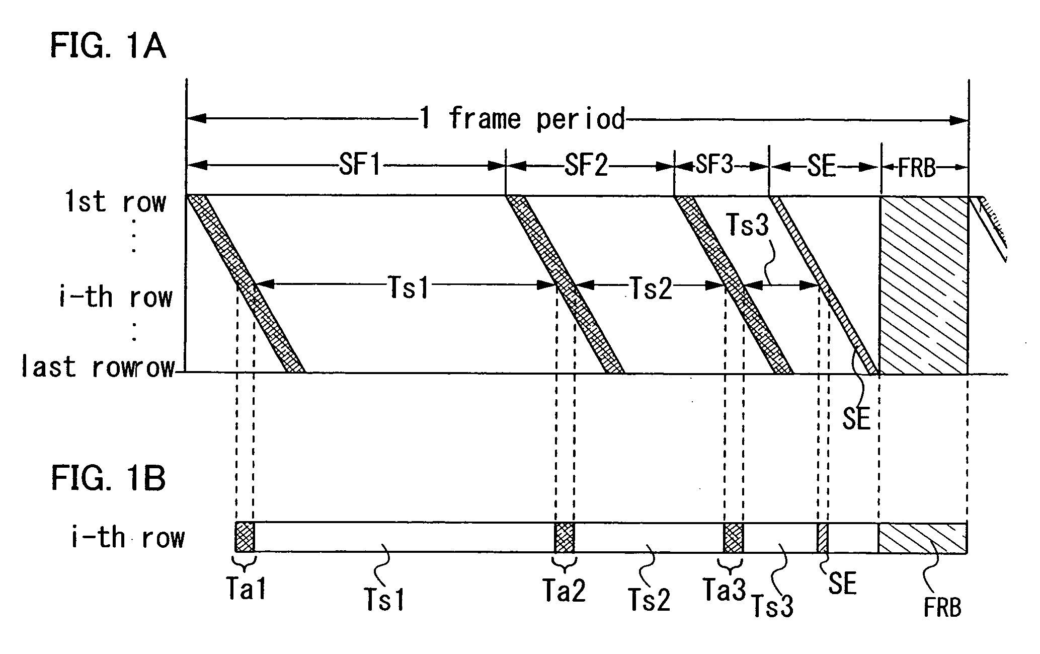
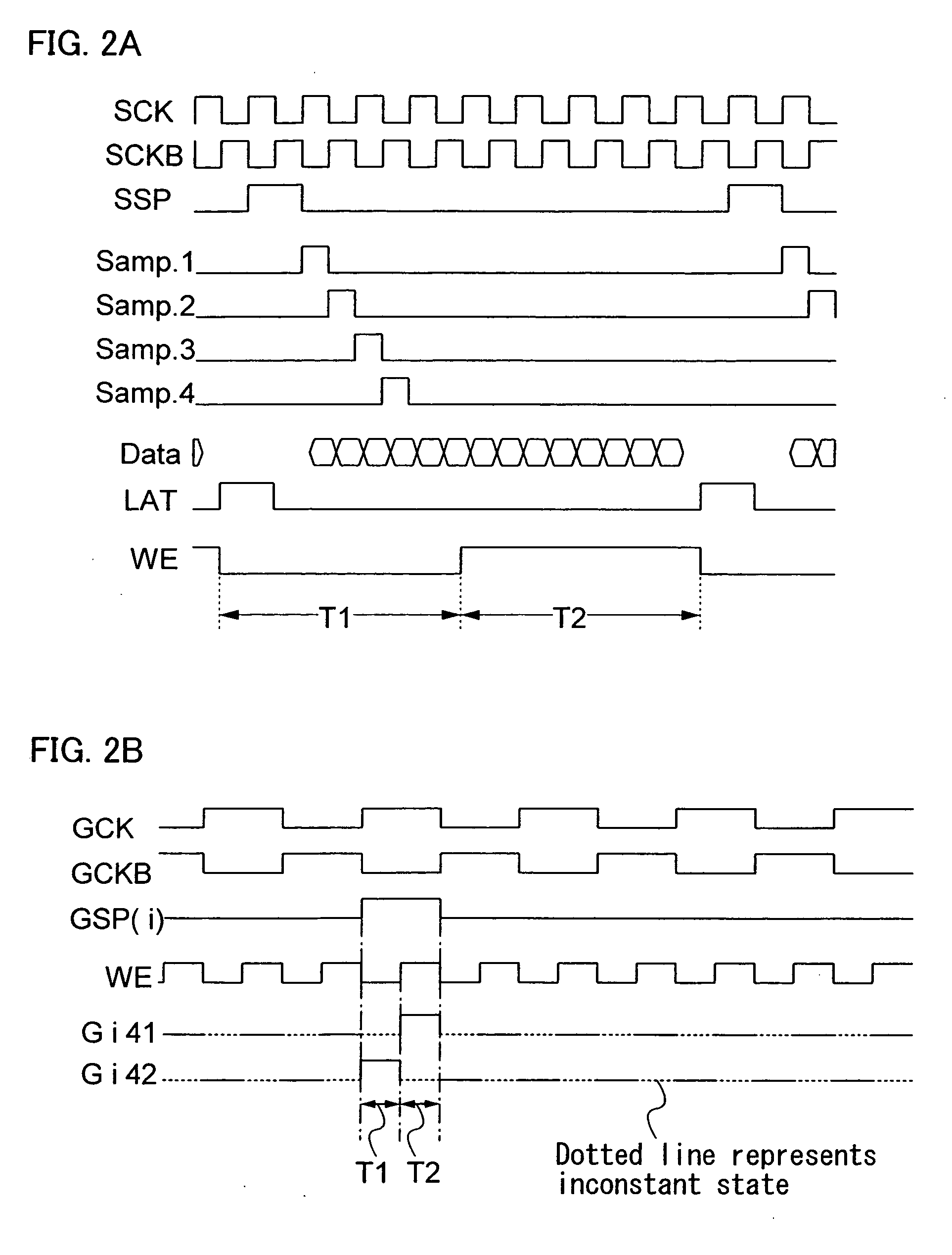
[0050] As to a light emitting device, the steps of depositing a light emitting layer material and sealing are performed after completing the step of manufacturing a TFT. The light emitting device in this state is referred to as a light emitting module. In the light emitting module, a wiring for inputting an external signal is connected to a display panel which is provided with each element. Thereafter, the light emitting module is subjected to aging for a certain period, mounted on a product, and then completed as a light emitting device. In this embodiment mode, drive employed for aging (aging drive) is explained below.

[0051] In this embodiment mode, a time gray scale method in which one frame period is divided into a plurality of subframe periods is applied to the aging drive. Forward voltage can be applied, and in addition, reverse voltage can also be applied. Note that, if voltage applied to make a light emitting element emit light is referred to as forward voltage, applying re...

embodiment mode 2

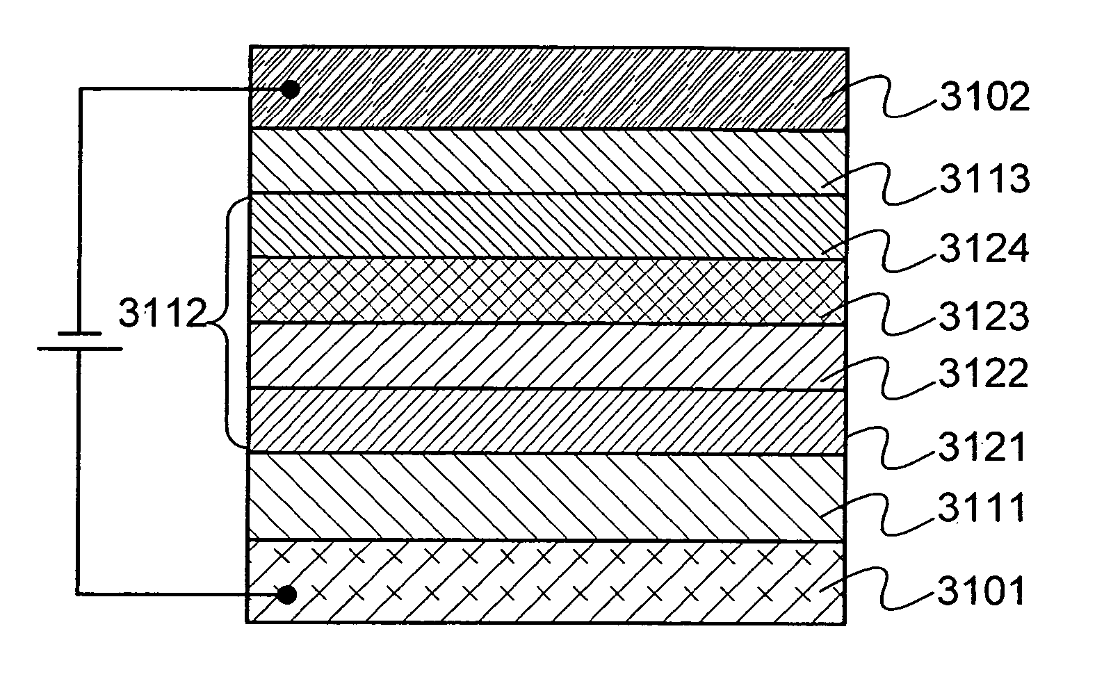
[0066] The present invention may further have a function of correcting for deterioration in a light emitting element after mounting on a product. Thus, explained in this embodiment mode is a structure of a display panel in a light emitting module mounted with a monitor circuit which serves to correct for deterioration in the light emitting element. Note that an active type light emitting device is described in this embodiment mode.

[0067] In FIG. 3, a pixel portion 40, a signal line driver circuit 43, a first scanning line driver circuit 41, a second scanning line driver circuit 42, and a monitor circuit 64 are provided over an insulating substrate.

[0068] The pixel portion 40 is provided with a plurality of pixels 10, and each pixel is provided with a light emitting element 13 and a transistor 12 which is connected to the light emitting element 13 and has a function of controlling current supply (hereinafter referred to as a driver transistor). The light emitting element is connect...

embodiment mode 3

[0095] In the invention, after mounting the light emitting module on a product, reverse voltage in addition to forward voltage may be applied to the light emitting element 13 and the monitor light emitting element 66. Thus, the case of applying reverse voltage after mounting the light emitting module is explained in this embodiment mode.

[0096] Explanation is made using the monitor light emitting element66. In order to apply reverse voltage, anode and cathode potentials of the monitor light emitting element are interchanged. Therefore, a potential of the monitor line 113 is made lower than that of the power source 18. As well as the light emitting element 13, in order to apply reverse voltage, anode and cathode potentials may be interchanged.

[0097] At this time, the cathode potential is preferably reversed after reversing the anode potential in the light emitting element 13 and the monitor light emitting element 66. After a predetermined reverse voltage period, the anode potential ...


PUM


Abstract

An object of the present invention is to provide a new light emitting element with little initial deterioration, and a display device in which initial deterioration is reduced and variation in deterioration over time is reduced by a new method for driving a display device having the light emitting element. One feature of the invention is that a display device comprising a light emitting element including a first electrode, a second electrode opposed to the first electrode, and a mixed layer of metal oxide and an organic compound provided between the first electrode and the second electrode is subjected to aging drive.

Description

BACKGROUND OF THE INVENTION [0001] 1. Field of the Invention [0002] The present invention relates to a method for manufacturing a light emitting device which has a highly stable light emitting element and in which the influence of variations in the light emitting element is reduced. [0003] 2. Description of the Related Art [0004] A display device using a light emitting element has the advantage of a wide viewing angle, high-speed response, low power consumption, or the like over that having a liquid crystal layer, and it is under development. [0005] A short circuit occurs in some cases in a portion between electrodes included in the element depending on manufacturing conditions. Then, electric current flows intensively into the short circuit portion. At this time, a current does not flow to other regions and the light emitting element is put into a non-light-emitting state as a whole, which results in a defect. [0006] A method is therefore proposed which does not damage a normal por...

Claims


Application Information

Patent Timeline
Patent Type & Authority Applications(United States)
IPC IPC(8): H01L31/12H05B44/00
CPCG09G3/007G09G3/2022G09G3/3258G09G2300/0819G09G2300/0842G09G2310/0251H01L2251/562G09G2310/027G09G2320/029G09G2320/043G09G2330/08H01L51/5265G09G2310/0256Y02B10/10H10K50/852H10K71/831H05B33/10
Inventor YAMAZAKI, SHUNPEIHAYAKAWA, MASAHIKOKAMATA, KOICHIROTOMATSU, HIROYUKIIKEDA, HISAOSAKATA, JUNICHIRO
Owner SEMICON ENERGY LAB CO LTD
Why Eureka
Try Eureka