Charge-pump-type power supply circuit

a power supply circuit and charge-pump technology, applied in the direction of process and machine control, instruments, machines without intermediate ac conversion, etc., can solve the problems of deteriorating an efficiency of the power supply, increasing the circuit size,

Inactive Publication Date: 2006-06-01
RENESAS TECH CORP
View PDF8 Cites 77 Cited by
  • Summary
  • Abstract
  • Description
  • Claims
  • Application Information

AI Technical Summary

Problems solved by technology

Therefore, the circuit needs to be formed with an element that can withstand the maximum input voltage, which results in an increase in a circuit size.
However, because this structure considerably deteriorates an efficiency of the power supply.

Method used


Image

  • Charge-pump-type power supply circuit
  • Charge-pump-type power supply circuit
  • Charge-pump-type power supply circuit

Examples


first embodiment

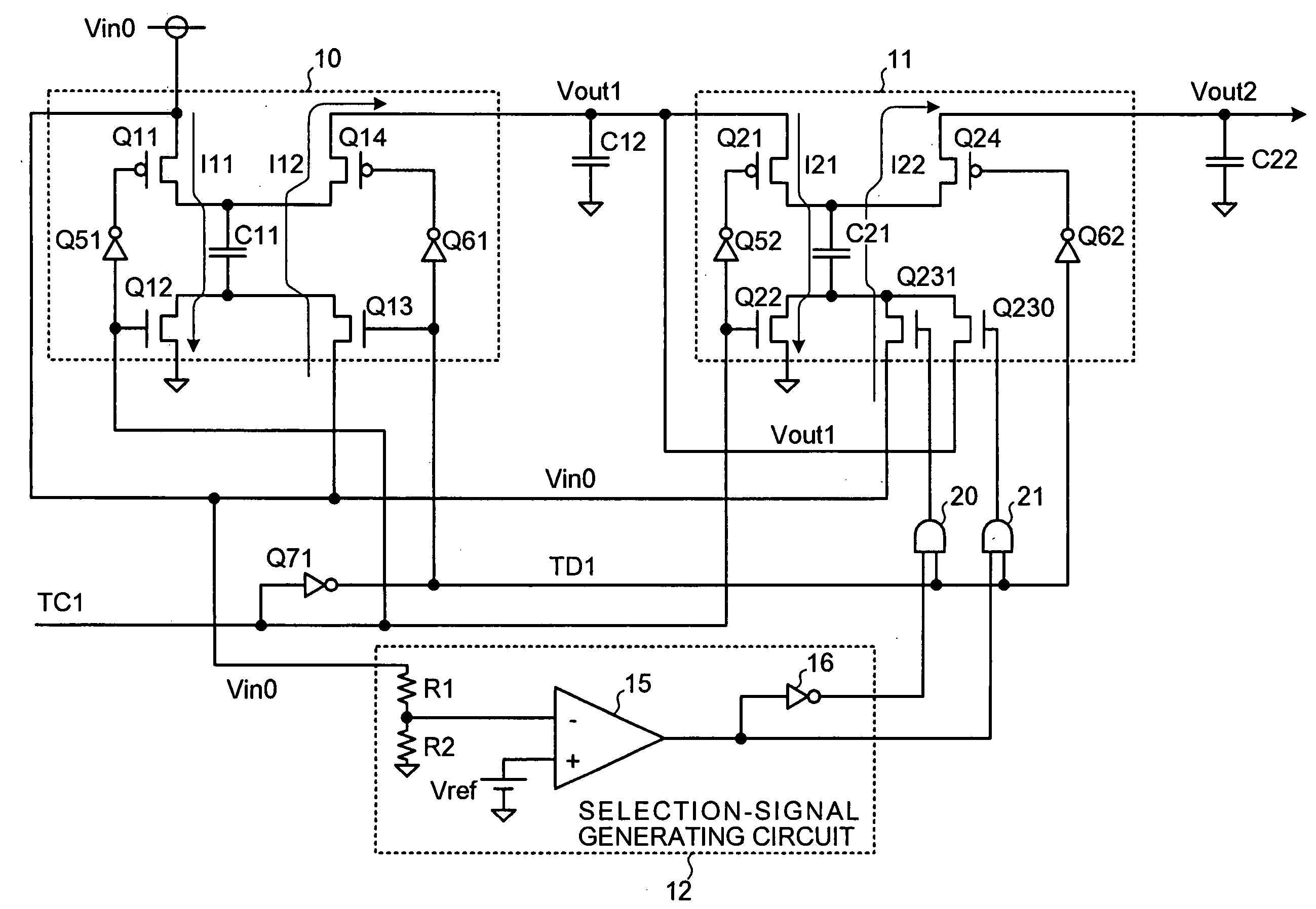
[0037]FIG. 1 is a circuit diagram of a charge-pump-type power supply circuit according to the present invention, with an example of a two-stage-cascaded charge-pump-type power supply circuit. Note that, in FIG. 1, the same or equivalent components as those shown in FIG. 8 are referred to by the same reference numerals. The input power-supply voltage is indicated by Vin0 instead of Vin.

[0038] A first-stage charge pump circuit 10 corresponds to the charge pump circuit CP1 shown in FIG. 8, and the second-stage charge pump circuit 11 corresponds to the charge pump circuit CP2, in which the NMOS transistor Q23 on the discharging side is replaced by two NMOS transistors Q230, Q231 connected in parallel. The power supply circuit shown in FIG. 1 also includes a selection-signal generating circuit 12, and AND circuits 20, 21 forming a selection circuit.

[0039] An output voltage Vout1 from the first-stage charge pump circuit 10 is applied to a source of the NMOS transistor Q230, while the inp...

second embodiment

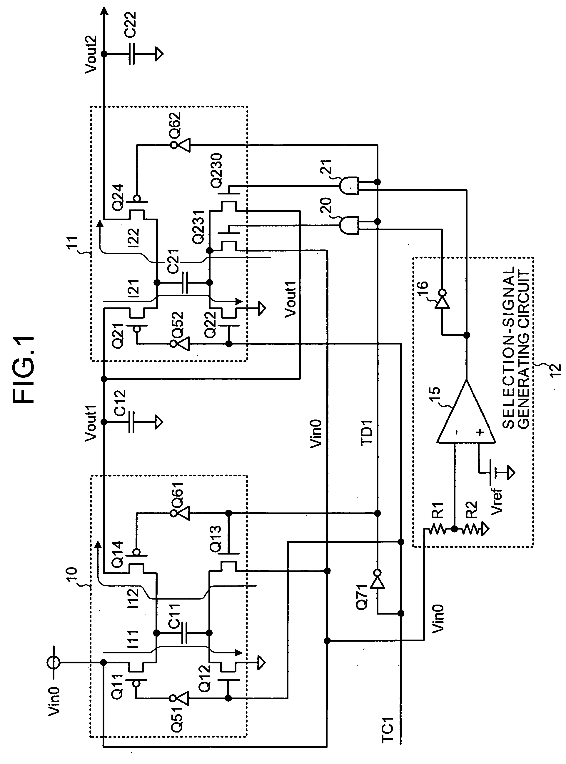
[0047]FIG. 2 is a circuit diagram of a charge-pump-type power supply circuit according to the present invention. In FIG. 2, the same or equivalent components as those shown in FIG. 8 and FIG. 1 are referred to by the same reference numerals.

[0048] As shown in FIG. 2, the charge-pump-type power supply circuit according to the second embodiment includes a second-stage charge pump circuit 25 as a second-stage charge pump circuit instead of the second-stage charge pump circuit 11 shown in FIG. 1. The second-stage charge pump circuit 25 corresponds to the charge pump circuit CP2 shown in FIG. 8 in which the PMOS transistor Q21 on the charging side is replaced by two PMOS transistors Q210, Q211 connected in parallel.

[0049] The output voltage Vout1 from the first-stage charge pump circuit 10 is applied to a source of the PMOS transistor Q210. The input voltage Vin0 is applied to a source of the NMOS transistor Q211.

[0050] The charging control signal TC1 is applied to the AND circuit 20, ...

third embodiment

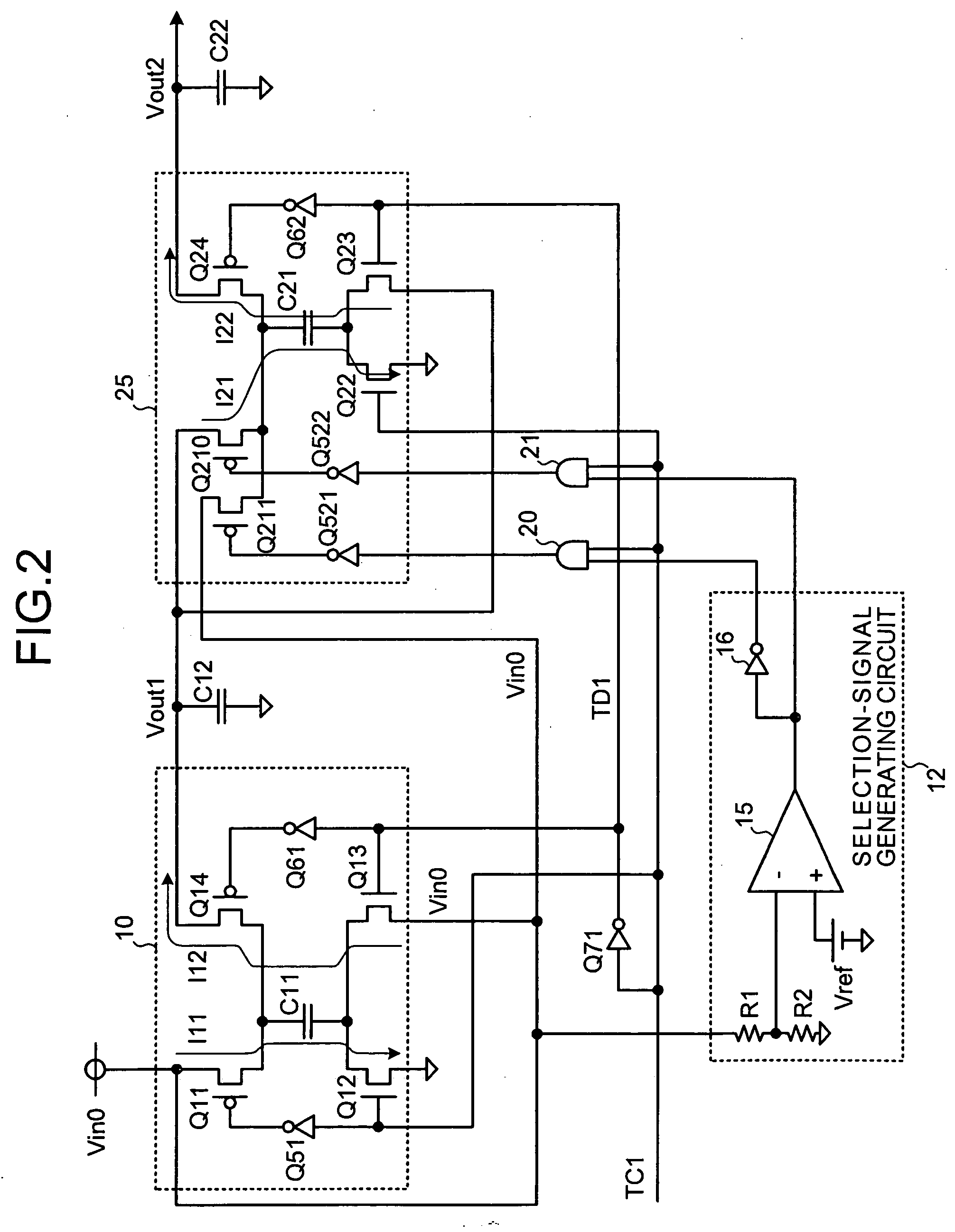
[0056]FIG. 3 is a circuit diagram of a charge-pump-type power supply circuit according to the present invention. In FIG. 3, the same or equivalent components as those shown in FIG. 1 are referred to by the same reference numerals.

[0057] In the charge-pump-type power supply circuit according to the third embodiment, the voltage dividing circuit (R1, R2) of the selection-signal generating circuit 12 monitors the output voltage Vout1 of the first-stage charge pump circuit 10 instead of the input voltage Vin0.

[0058] According to this configuration, the same operational advantage as in the first embodiment and the monitor voltage corresponds to twice the input voltage Vin0 are provided, which can double the inversion accuracy of the comparison circuit in the selection-signal generating circuit 12.


PUM


Abstract

Two charge pump circuits are connected in a cascade manner. Each of the charge pump circuits includes two charging switches and two voltage-boosting switches. A voltage-boosting switch, provided on a side for adding a boosting voltage to a charging voltage in a second-stage charge pump circuit, includes a plurality of switches. One ends of the switches are commonly connected to a capacitor. Different boosting voltages are applied to other ends of the switches. A selecting unit selects one of the switches, during a boosting period, based on an input voltage or an output voltage to or from a first-stage charge pump circuit.

Description

BACKGROUND OF THE INVENTION [0001] 1. Field of the Invention [0002] The present invention relates to a charge-pump-type power supply circuit that boosts an input voltage with charging and discharging of a capacitor, and more particularly, to a charge-pump-type power supply circuit that can obtain a high voltage by a multistage cascaded-connection. [0003] 2. Description of the Related Art [0004] Generally, a charge-pump-type power supply circuit uses a metal-oxide semiconductor (MOS) transistor for a switch forming a charging path and a discharging path, and boosts a voltage by applying an input voltage to a charging capacitor through the charging path to accumulate charges, applying the input voltage to the charging capacitor through the discharging path to add charges to the accumulated charges, and transferring total charges to an output capacitor. A conventional charge-pump-type power supply circuit is disclosed in, for example, Japanese application patent laid-open publication N...

Claims


Application Information

Patent Timeline
Patent Type & Authority Applications(United States)
IPC IPC(8): G05F1/10
CPCH02M3/07
Inventor SOHARA, YASUYUKITANAKA, MASAYASU
Owner RENESAS TECH CORP
Why Eureka
Try Eureka