Display device

a display device and display technology, applied in the field of display devices, can solve the problems of increasing production costs, signal delay, and complicat achieve the effects of simplifying the manufacturing process, reducing cost, and reducing the number of data driving ic chips

Active Publication Date: 2006-06-08
SAMSUNG DISPLAY CO LTD
View PDF16 Cites 102 Cited by
  • Summary
  • Abstract
  • Description
  • Claims
  • Application Information

AI Technical Summary

Benefits of technology

[0013] This invention provides a display device having an arrangement of switching elements of pixels arranged on a substrate thereof that allows for a driving scheme that reduces the number of data driving IC chips while ensuring image quality; thereby simplifying a manufacturing process and reducing cost.

Problems solved by technology

In particular, the number of the data driving IC chips is important since the data driving IC chips are much more expensive than the gate driving IC chips.
However, the polarity inversion of the data voltages flowing in each data line often requires complicated driving scheme that may cause signal delay.
Although the signal delay may be reduced by using a low resistivity metal, it may complicate the manufacturing process and increase the production cost.
However, the column inversion technique is inferior to the dot inversion technique in terms of vertical crosstalk and vertical flickering, etc.

Method used


Image

  • Display device
  • Display device
  • Display device

Examples


Embodiment Construction

[0028] The present invention is described more fully below with reference to the accompanying drawings, in which preferred embodiments of the invention are shown. This invention may, however, be embodied in many different forms and should not be construed as limited to the embodiments set forth herein. Like numerals refer to like elements throughout.

[0029] In the drawings, the thickness of layers and regions are exaggerated for clarity. Like numerals refer to like elements throughout. It will be understood that when an element such as a layer, region or substrate is referred to as being “on” another element, the element may be directly on the other element or intervening elements may also be present. In contrast, when an element is referred to as being “directly on” another element, there are no intervening elements present.

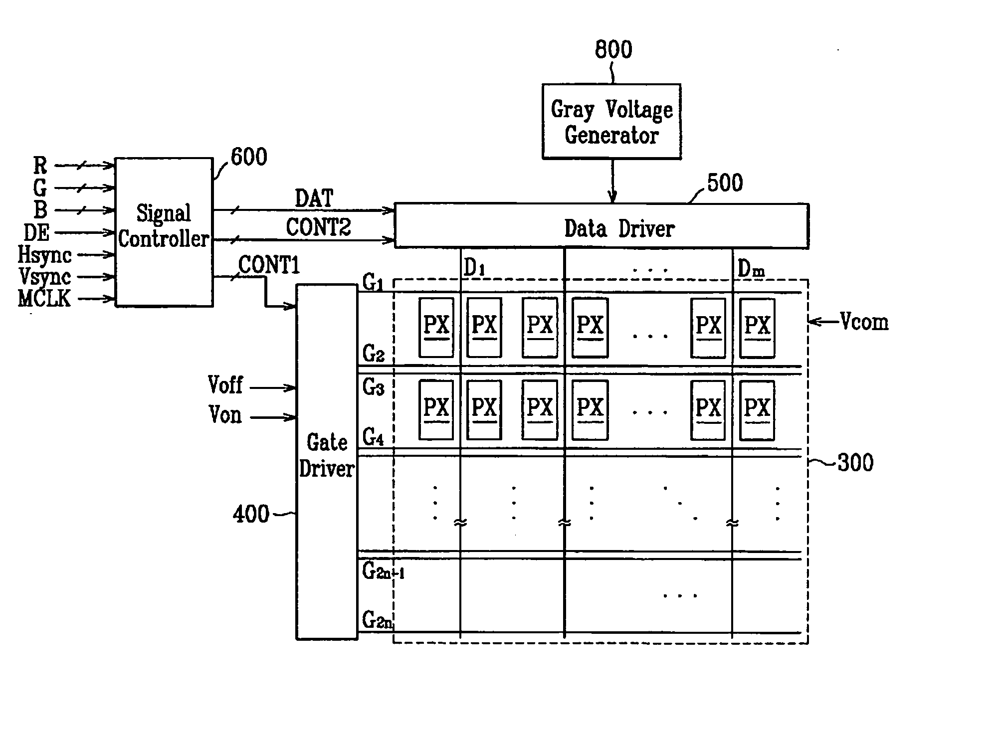
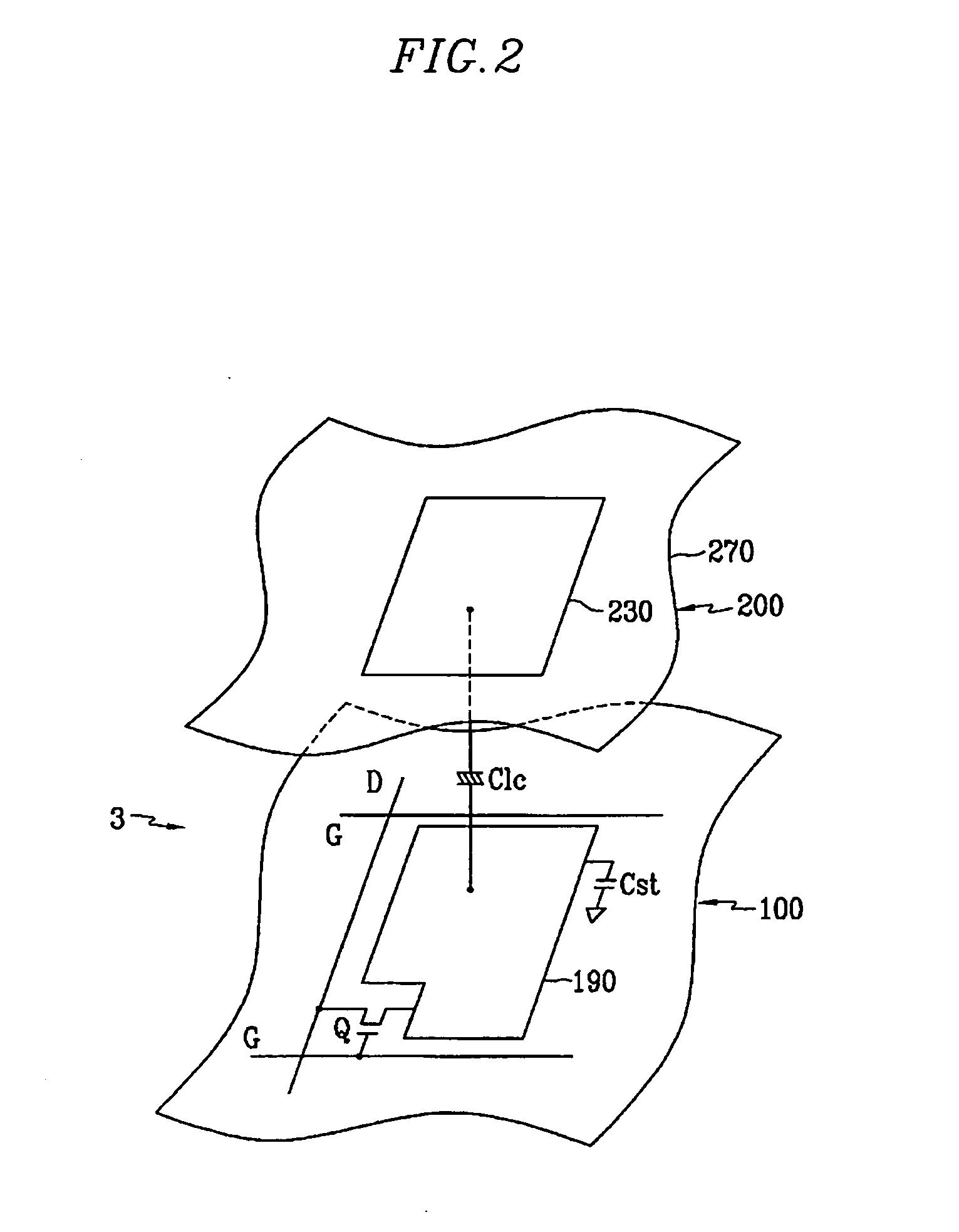
[0030] Liquid crystal displays (LCD) as an example of a display device according to embodiments of the invention are described below with reference to the acco...


PUM


Abstract

A display device including a plurality of pixel electrodes arranged in a matrix including rows and columns and a plurality switching elements coupled with the pixel electrodes; a plurality of gate lines coupled with the switching elements and extending in a row direction, at least two gate lines assigned to a row; and a plurality of data lines coupled with the switching elements and extending in a column direction, a data line assigned to at least two columns, wherein each of the pixel electrodes has a first side and a second side that is farther from a data line than the first side, and the switching elements are disposed near the second sides of the pixel electrodes.

Description

CROSS REFERENCE TO RELATED APPLICATIONS [0001] This application claims priority to and the benefit of Korean Patent Application No. 10-2004-0072507 filed on Sep. 10, 2004, Korean Patent Application No. 10-2004-0072749 filed on Sep. 10, 2004, and Korean Patent Application No. 10-2004-0072685 filed on Sep. 10, 2004, which are hereby incorporated by reference for all purposes as if fully set forth herein. BACKGROUND OF THE INVENTION [0002] 1. Field of the Invention [0003] The present invention relates to a display device having an improved structure and driving scheme that simplifies manufacturing processes and reduces cost. [0004] 2. Description of Related Art [0005] An active type display device such as an active matrix (AM) liquid crystal display (LCD) and an active matrix organic light emitting display (OLED) includes a plurality of pixels arranged in a matrix and including switching elements and a plurality of signal lines such as gate lines and data lines for transmitting signals...

Claims


Application Information

Patent Timeline
Patent Type & Authority Applications(United States)
IPC IPC(8): G11C11/34G11C16/06
CPCG02F1/1368G09G3/3614G09G3/3648G09G3/3677G09G3/3688G09G2300/0426G09G2310/0262
Inventor PARK, HAENG-WONLEE, SEONG-YOUNGLEE, YONG-SOONKANG, NAM-SOOMOON, SEUNG-HWANLEE, BONG-JUNKIM, SUNG-MANKIM, BEOM-JUNMOON, YEON-KYUPARK, HYEONG-JUNKANG, SHIN-TACK
Owner SAMSUNG DISPLAY CO LTD
Why Eureka
Try Eureka