Method for reducing line edge roughness for conductive features

a technology of conductive features and line edges, which is applied in the direction of basic electric elements, electrical apparatus, semiconductor devices, etc., can solve the problems of shortening the maturation period of a particular photoresist chemistry, less uniform resistance, and reducing the reliability of the completed semiconductor devi

Active Publication Date: 2006-06-08
TEXAS INSTR INC
View PDF13 Cites 11 Cited by
  • Summary
  • Abstract
  • Description
  • Claims
  • Application Information

AI Technical Summary

Problems solved by technology

However, maturation of a particular photoresist chemistry may be long compared to the design cycle of the industry, forcing manufacturers to go to production with a resist that has not yet been fully optimized with respect to LER.
This is particularly a probl...

Method used


Image

  • Method for reducing line edge roughness for conductive features
  • Method for reducing line edge roughness for conductive features
  • Method for reducing line edge roughness for conductive features

Examples


Embodiment Construction

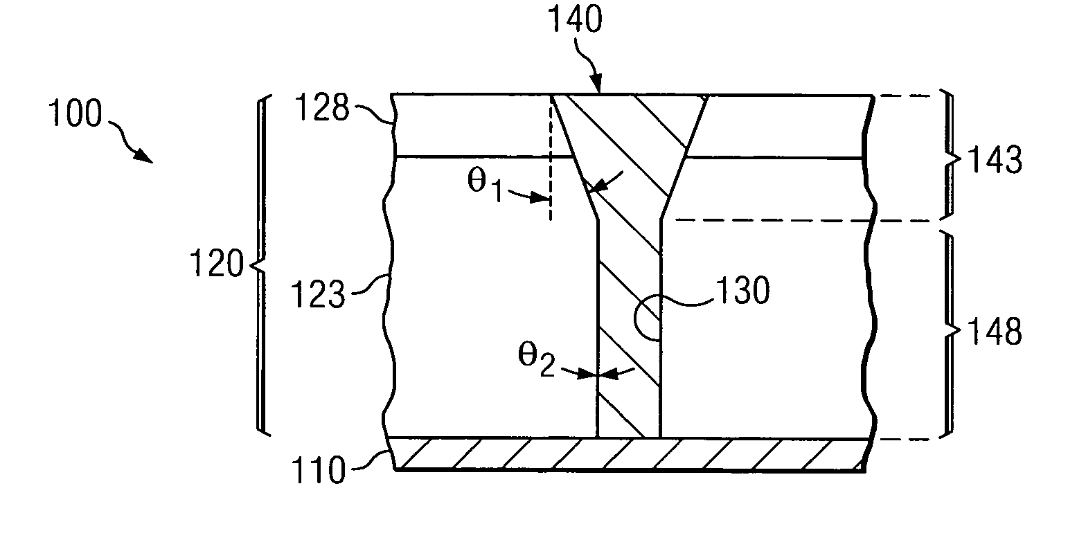
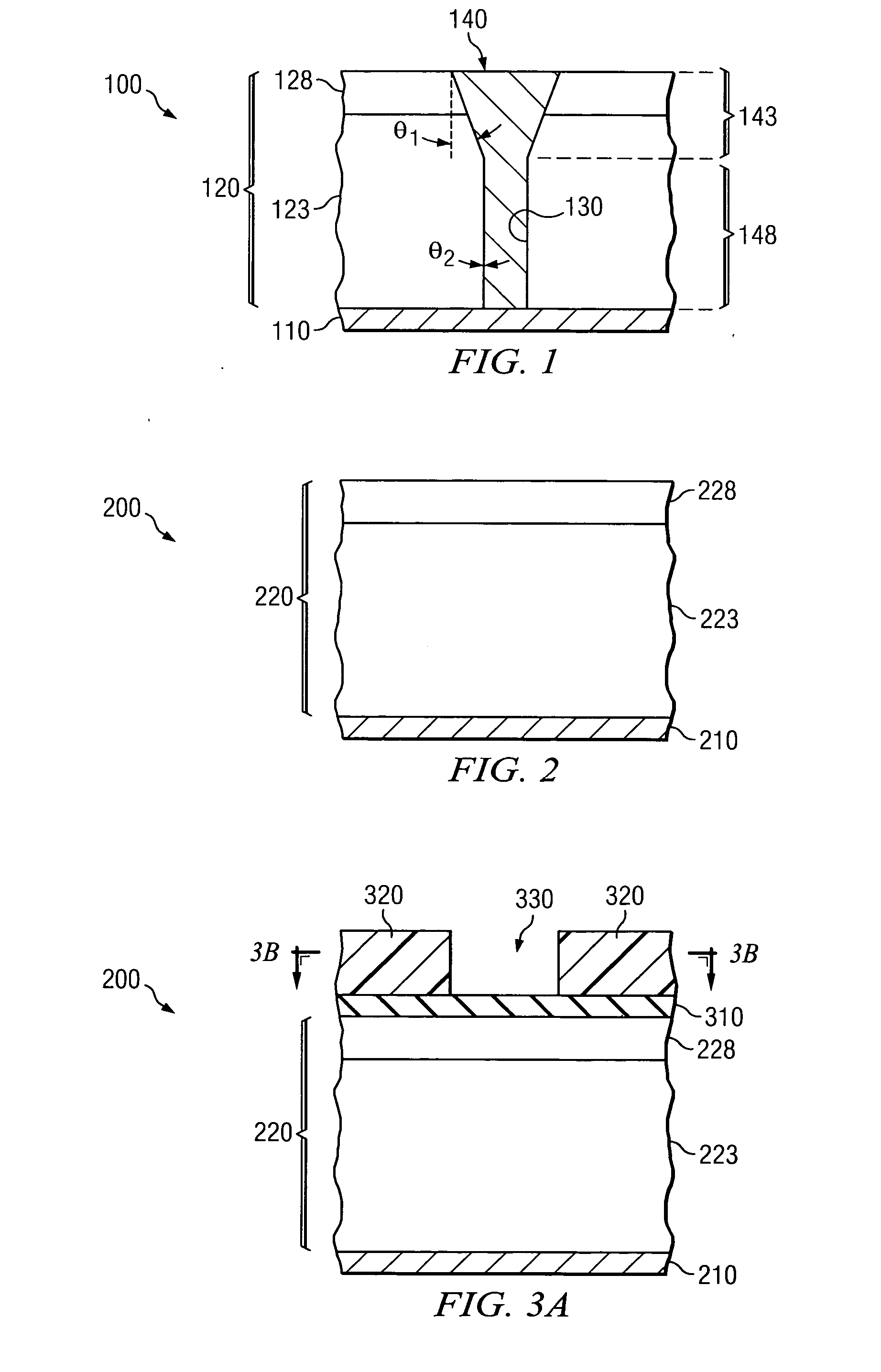
[0029] Referring initially to FIG. 1, illustrated is a cross-sectional view of a semiconductor feature, such as an interconnect structure 100, which has been manufactured in accordance with the principles of the present invention. The interconnect structure 100 illustrated in FIG. 1 includes a conductive feature 110. The conductive feature 110 may comprise a number of different features while remaining within the scope of the present invention. In one aspect of the invention, the conductive feature 110 is a transistor device level feature, such as a gate electrode or source / drain contact region. In another aspect, however, the conductive feature 110 is a conductive trace or runner traversing along at least a portion of an interlevel dielectric layer. Other conductive features 110 may also exist.

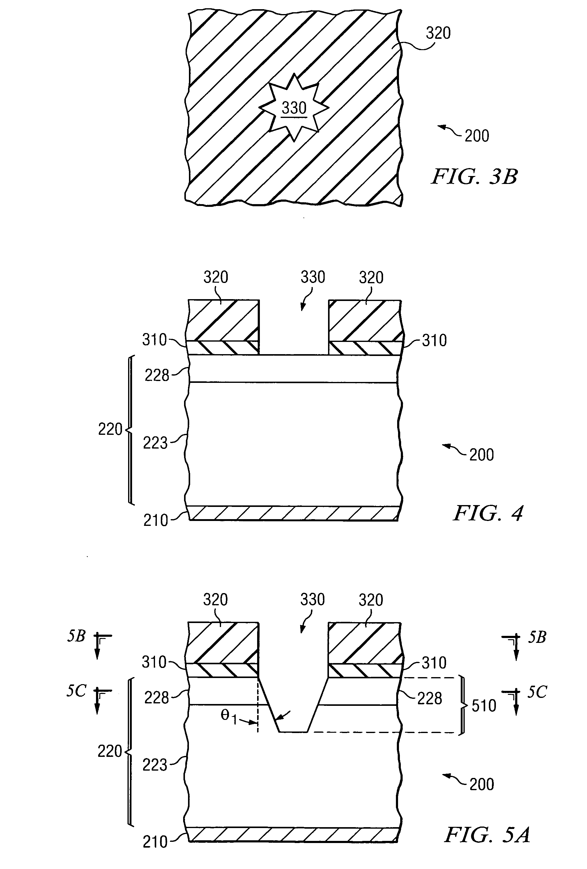
[0030] Located over the conductive feature 110 is a substrate, such as a dielectric layer 120. Similar to the conductive feature 110, the dielectric layer 120 may comprise a variety of dif...


PUM

PropertyMeasurementUnit
Angleaaaaaaaaaa
Angleaaaaaaaaaa
Fractionaaaaaaaaaa

Abstract

The present invention provides an interconnect structure, a method of manufacture therefore, and a method for manufacturing an integrated circuit including the same. The method for forming the interconnect structure, among other steps, includes subjecting a first portion (510) of a substrate (220) to a first etch process, the first etch process designed to etch at a first entry angle (θ1), and subjecting a second portion (610) of the substrate (220) to a second different etch process, the second different etch process designed to etch at a second lesser entry angle (θ2).

Description

CROSS REFERENCE TO PROVISIONAL APPLICATION [0001] This application claims the benefit of U.S. Provisional Application No. 60 / 632,407 entitled “LINE EDGE ROUGHNESS REDUCTION AT THE 90 nm TECHNOLOGY NODE FOR CONTACT AND TRENCH ETCHED FEATURES,” to David G. Farber, et al, filed on Dec. 2, 2004, which is commonly assigned with the present invention and incorporated herein by reference as if reproduced herein in its entirety.TECHNICAL FIELD OF THE INVENTION [0002] The present invention is directed, in general, to a method for forming openings in a substrate and, more specifically, to a method for reducing line edge roughness for conductive features in a substrate. BACKGROUND OF THE INVENTION [0003] Integrated circuits are mass-produced by fabricating hundreds of identical circuit patterns on a single semiconductor wafer. One of the many different processes repeated over and over in manufacturing these integrated circuits is that of using a mask and etchant for forming a particular featur...

Claims


Application Information

Patent Timeline
IPC IPC(8): H01L21/311H01L21/302
CPCH01L21/31116H01L21/76804H01L21/76816
Inventor FARBER, DAVID G.GOODLLIN, BRIAN E.KRAFT, ROBERT
Owner TEXAS INSTR INC
Why Eureka
Try Eureka