Mask for forming landing plug contact hole and plug forming method using the same
a technology of contact hole and mask, which is applied in the field of mask for forming contact hole of landing plug and plug forming method using the same, can solve the problems of affecting the forming efficiency of the contact hole,
- Summary
- Abstract
- Description
- Claims
- Application Information
AI Technical Summary
Benefits of technology
Problems solved by technology
Method used
Image

Examples
Embodiment Construction
[0030] Now, a preferred embodiment of the present invention will be explained in detail to be easily understood by those skilled in the art with reference of the accompanying drawings.
[0031] In the drawings, thicknesses of respective layers and regions are exaggerated for clarity of understanding, and like reference numerals refer to like elements throughout.
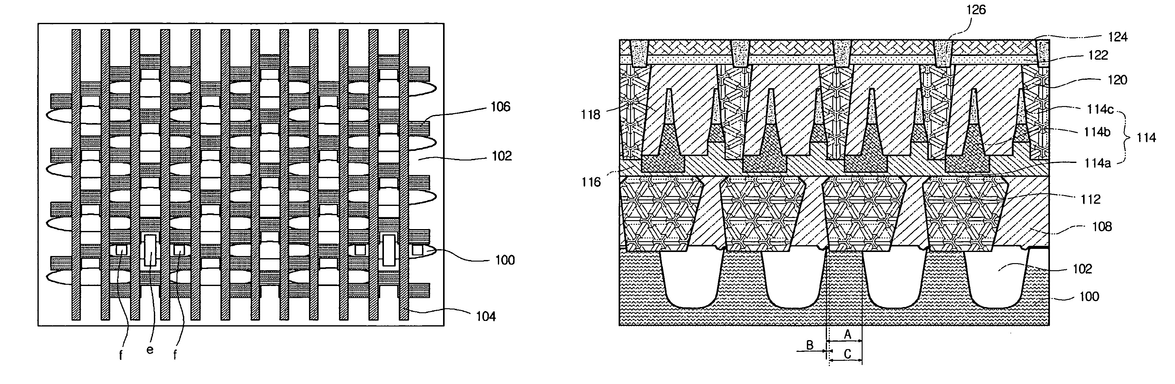
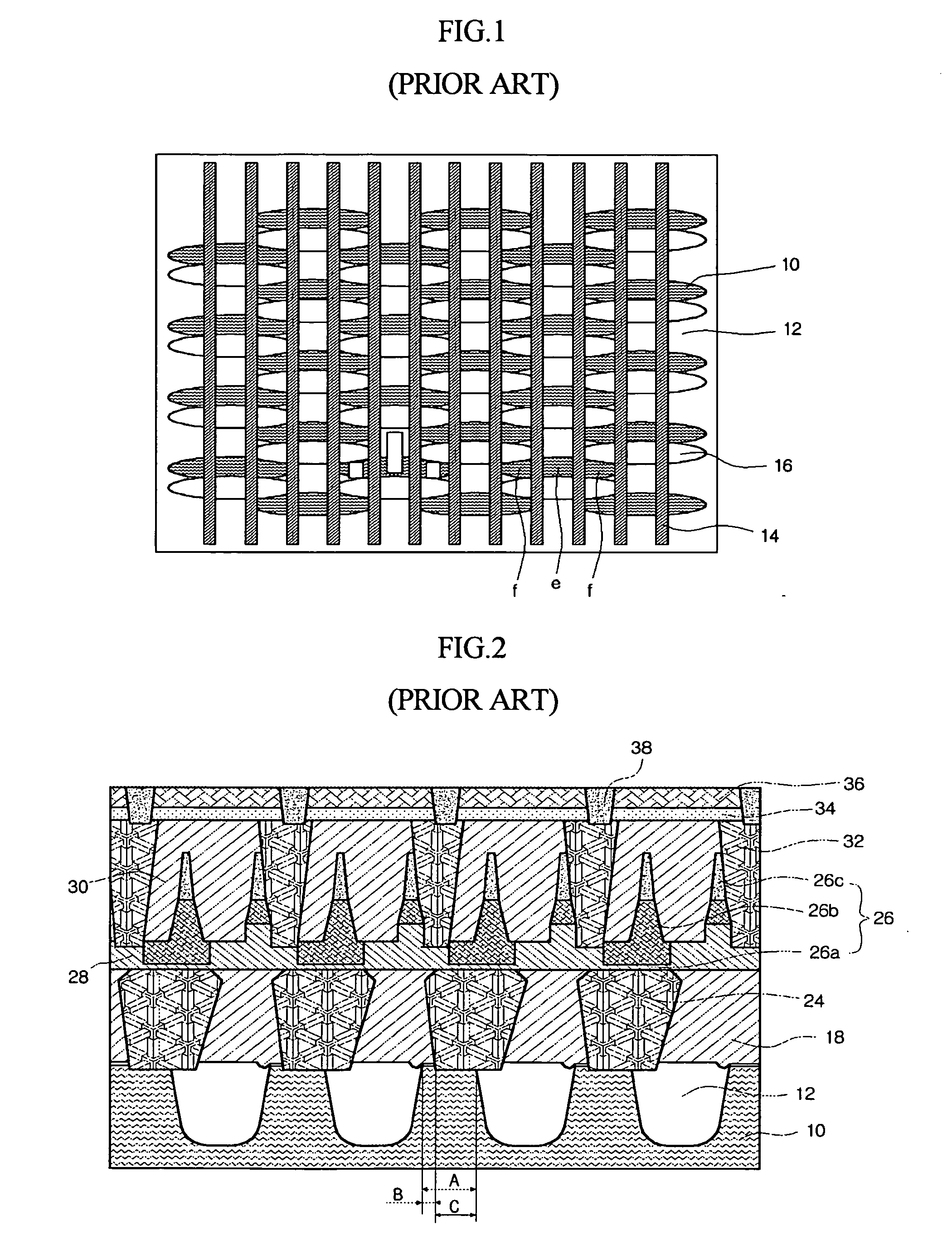
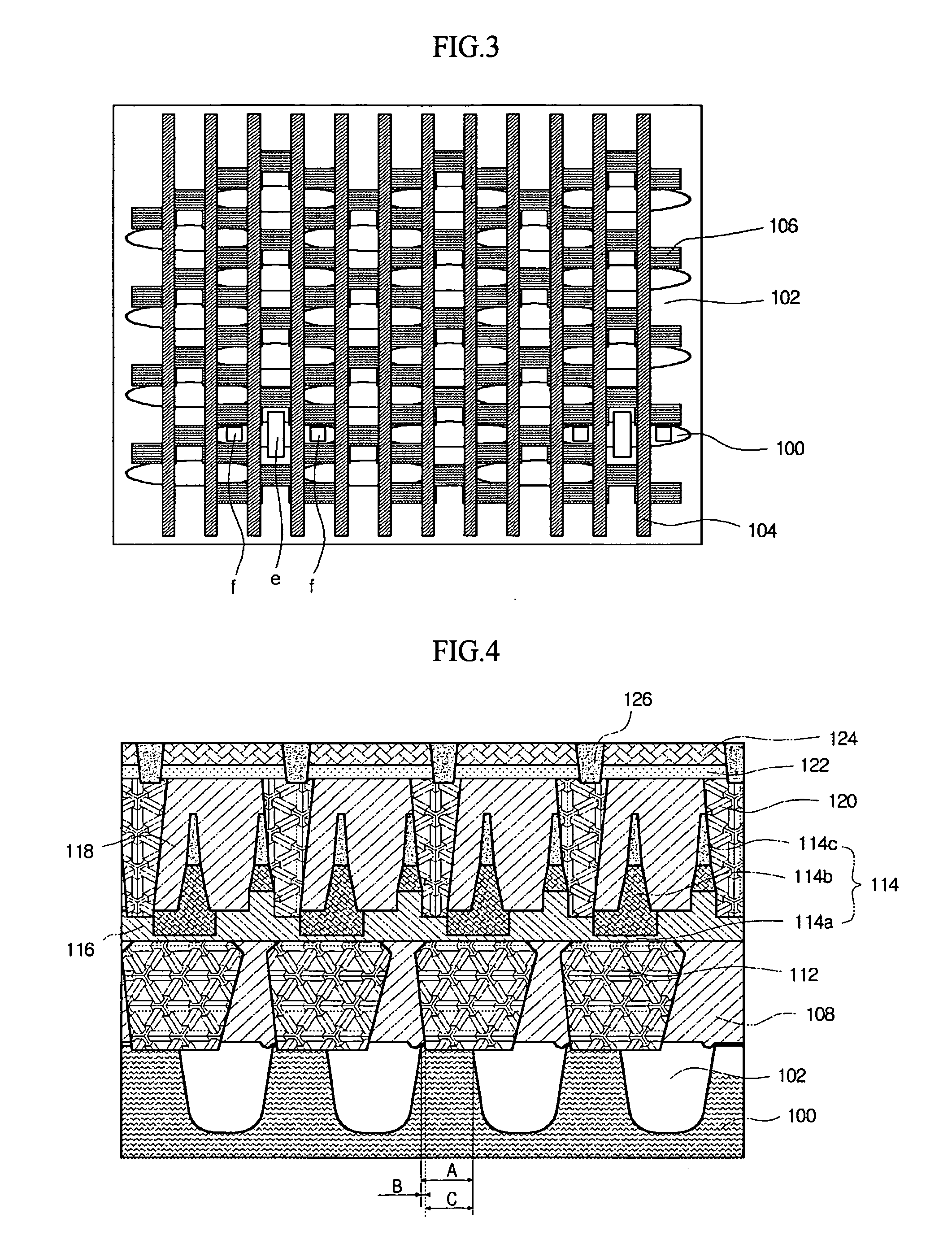
[0032]FIG. 3 is a plan view illustrating a mask pattern for forming landing plug contact holes in accordance with an embodiment of the present invention.
[0033] As shown in FIG. 3, a semiconductor substrate, including device active regions 100 and device inactive regions 102, is prepared. The semiconductor substrate is provided with a cell transistor including a plurality of lines, i.e. gate electrodes 104. An inter-insulation layer (not shown) covers the overall upper surface of the semiconductor substrate formed with the cell transistor. The active regions 10 between the gate electrodes 104 form contact areas e and f to be c...
PUM
 Abstract
Description
Claims
Application Information
 - R&D Engineer
- R&D Manager
- IP Professional
- Industry Leading Data Capabilities
- Powerful AI technology
- Patent DNA Extraction
Browse by: Latest US Patents, China's latest patents, Technical Efficacy Thesaurus, Application Domain, Technology Topic.
© 2024 PatSnap. All rights reserved.Legal|Privacy policy|Modern Slavery Act Transparency Statement|Sitemap