Method for fabricating bulb-shaped recess pattern

a recess pattern and bulb-shaped technology, applied in the direction of semiconductor devices, electrical appliances, basic electric elements, etc., can solve the problems of degrading the refresh property of the device, ficd, and difficulty in defining a line width with less than 30 nm, so as to reduce the increase of a critical dimension, reduce the shift of the seam, and increase the seam. effect of bias

Inactive Publication Date: 2010-07-06
SK HYNIX INC
View PDF24 Cites 2 Cited by
  • Summary
  • Abstract
  • Description
  • Claims
  • Application Information

AI Technical Summary

Benefits of technology

[0014]Embodiments of the present invention are directed toward providing a method for fabricating a bulb-shaped recess gate, wherein the method can reduce an increase in a bias of a critical dimension, bowing and sloped profiles, a top attack, a ball-not-defined phenomenon, an increase in a seam and a shift of the seam.

Problems solved by technology

However, it is difficult to define a line width with less than 30 nm for patterning.
Furthermore, if a bias level of a recess etch is increased, it becomes impossible to control the line width by less than 30 nm to satisfy a final inspection critical dimension (FICD).
As a result, a refresh property of a device may be degraded.
As the design rule has been reduced, a bottom profile of the recess gate is deteriorated and thus, an electric field is increased.
Also, since the HTO layer is excessively formed at a bottom portion because of a difference in a deposition rate on a surface where the spacers are to be formed, a ball pattern may not be formed.
If the excessive etch is performed, a top attack of the bulb-shaped recess is generated.
The shift of the seam 23 may degrade reliability of the device.

Method used


Image

  • Method for fabricating bulb-shaped recess pattern
  • Method for fabricating bulb-shaped recess pattern
  • Method for fabricating bulb-shaped recess pattern

Examples


Embodiment Construction

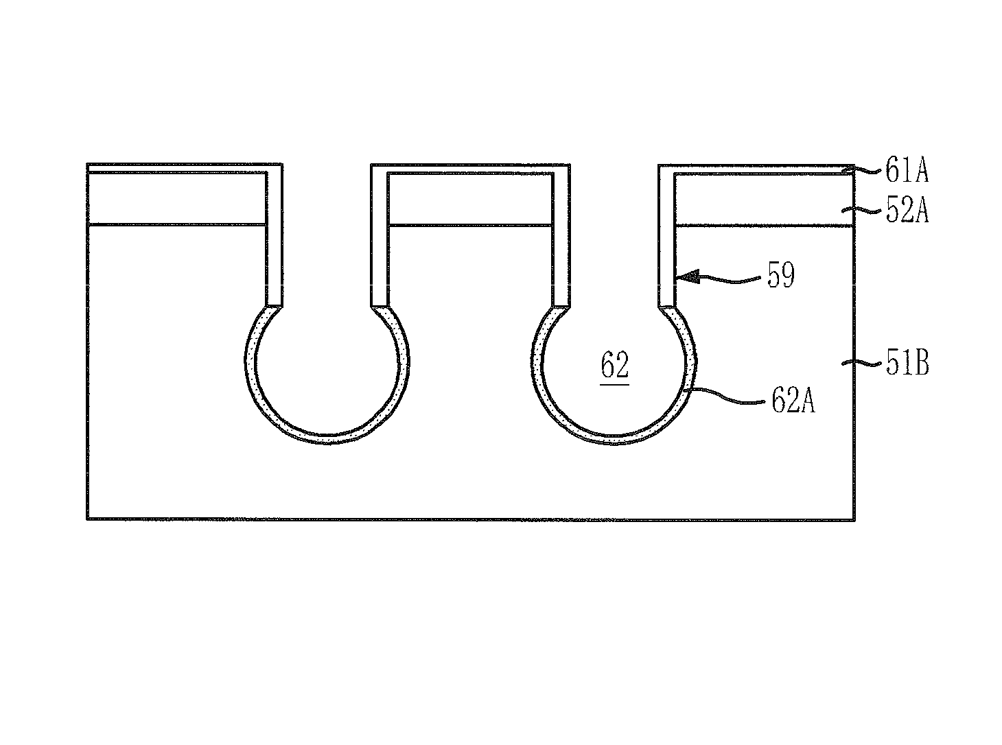
[0026]Turning now to the drawings, FIGS. 4A to 4H illustrate a method for fabricating a bulb-shaped recess pattern in accordance with an embodiment of the present invention. As shown in FIG. 4A, an etch barrier layer 32 is formed over a substrate 31 in which an active region is defined. The etch barrier layer 32 serves as an etch barrier during an etching process to form a subsequent ball pattern. The etch barrier layer 32 includes an oxide layer.

[0027]A hard mask layer 100 required to perform a recess etch is formed over the etch barrier layer 32. The hard mask layer 100 is formed by stacking an amorphous carbon layer 33 and a silicon oxynitride (SiON) layer 34, and combination thereof. The SiON layer 34 serves as an etch barrier during etching the amorphous carbon layer 33, and the amorphous carbon layer 33 serves as an etch barrier during etching the substrate 31 to form recesses.

[0028]An anti-reflective coating layer 35 is formed over the hard mask layer 100. Then, a photoresist...


PUM


Abstract

A method for fabricating a bulb-shaped recess pattern includes: forming an etch barrier layer over a substrate; forming a hard mask pattern in which a first polymer is attached to sidewalls of the hard mask pattern over the etch barrier layer; sequentially etching the etch barrier layer and the substrate to form a recess pattern in which a second polymer is attached to sidewalls of the recess pattern; removing the first and second polymers and the hard mask pattern; forming a plurality of spacers exposing a bottom portion of the recess pattern; and etching the exposed bottom portion of the recess pattern to form a ball pattern.

Description

CROSS-REFERENCE TO RELATED APPLICATIONS[0001]The present invention claims priority of Korean patent application number 10-2007-0000749, filed on Jan. 3, 2007 which is incorporated by reference in its entirety.FIELD OF THE INVENTION[0002]The present invention relates to a method for fabricating a semiconductor device, and more particularly, to a method for fabricating a bulb-shaped recess pattern used as a channel of a transistor.BACKGROUND OF THE INVENTION[0003]Recently, a recess pattern process using a recess channel has been suggested to secure a channel length of a transistor in fabricating a dynamic random access memory (DRAM) device. As a design rule of the DRAM device, a critical dimension (CD) of a recess gate should be controlled and reduced.[0004]However, it is difficult to define a line width with less than 30 nm for patterning. Furthermore, if a bias level of a recess etch is increased, it becomes impossible to control the line width by less than 30 nm to satisfy a final ...

Claims


Application Information

Patent Timeline
Patent Type & Authority Patents(United States)
IPC IPC(8): H01L21/302
CPCH01L21/3065H01L21/3086H01L21/31116H01L21/31122H01L29/4236H01L29/66621H01L21/18
Inventor KIM, MYUNG-OKKIM, TAE-HYOUNG
Owner SK HYNIX INC
Why Eureka
Try Eureka