System and method for shifting critical dimensions of patterned films

a technology of critical dimensions and patterned films, applied in the field of substrate patterning, can solve the problems of device defects, feature and structure creations that have undesirable critical dimensions (cds) or variations in cds, and achieve the effects of improving yield, fine tuning results, and improving uniformity

Active Publication Date: 2018-05-22
TOKYO ELECTRON LTD
View PDF35 Cites 2 Cited by
  • Summary
  • Abstract
  • Description
  • Claims
  • Application Information

AI Technical Summary

Benefits of technology

[0006]Techniques herein include systems and methods that provide a spatially-controlled projection of light or electromagnetic radiation (EMR) onto a substrate. This spatially-controlled light projection can selectively activate a portion of photoresist acid generators as either a pre-exposure dose or a post-exposure dose to fine tune critical dimensions created by a scanner, stepper, or other reticle-based exposure system. Combining such spatial light projection with lithographic exposure can achieve significant improvements in critical dimension uniformity across a surface of a substrate. Light projected can be of any wavelength such as 172 nm laser, 400-700 nm light, Ultra Violet Light (UV), Extreme Ultraviolet Light (EUV), Infrared light, 13.4 nm radiation, etc. A given projected image can comprise multiple intensities and various wavelengths or a substantially same wavelength, which can be set to change and maintain many different steady state conditions on multiple substrates simultaneously. In other words, a combination of a pre / post exposure pixel-based electromagnetic radiation treatment (projected image) in combination with lithographic reticle-based exposure can correct feature dimensions that would otherwise be unacceptable or cause defects.
[0008]The projected pattern of EMR can be tailored to specific results desired. For example, increasing or decreasing critical dimensions, facilitating edge bead removal, alignment mark reveal, EUV flare compensation, and so forth. Thus, a combination of fine and coarse control for a CD control can provide dramatically better uniformity and improve yield. Because light can alter material properties of certain materials (such as photoresists), existing exposures can be augmented to be biases up or down.
[0009]By way of a specific, non-limiting example, a projection system projects a pattern of EMR using a 172 nm laser or infrared laser the Critical Dimensions (CD) of a substrate can be changed to meet an engineer's needs by adding this process to the recipe queue. The 172 nm laser or infrared laser activates PAG anywhere on the substrate within the diameter of the 172 nm laser or infrared laser resolution. After running a substrate through a recipe any CDs that are out of required parameters can be recorded and then those CD corrections can be inputted into a new recipe with the addition of the critical dimension shifting process as described herein. This shifting process can be added before a primary exposure process (mask-based) or after the primary exposure process. As a new substrate is treated with pre-exposure techniques herein, the CD will be shifted in a specified region and the remaining recipe can be followed with the new CDs. This process allows for finer tuned results than is conventionally possible. Being able to adjust a CD of a substrate will increase efficiency and reduce semiconductor fabrication costs.

Problems solved by technology

Conventional photolithographic exposure techniques, however, are not perfect.
For example, features and structures created can have undesirable critical dimensions (CDs) or variations in CDs that are not desirable or within specified tolerances.
Such undesirable CDs can cause device defects or otherwise compromise performance.

Method used


Image

  • System and method for shifting critical dimensions of patterned films
  • System and method for shifting critical dimensions of patterned films
  • System and method for shifting critical dimensions of patterned films

Examples


Embodiment Construction

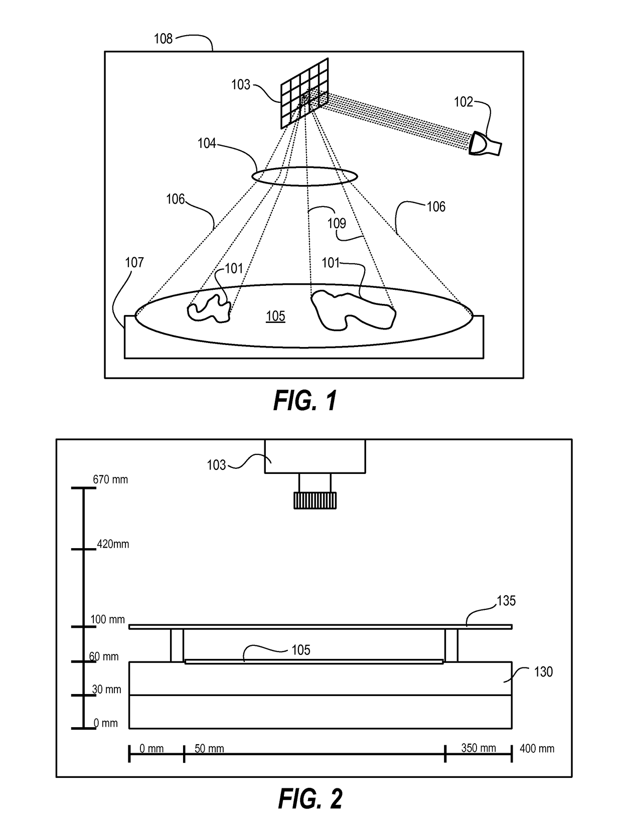
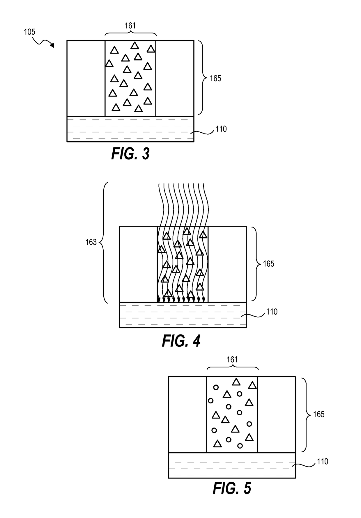
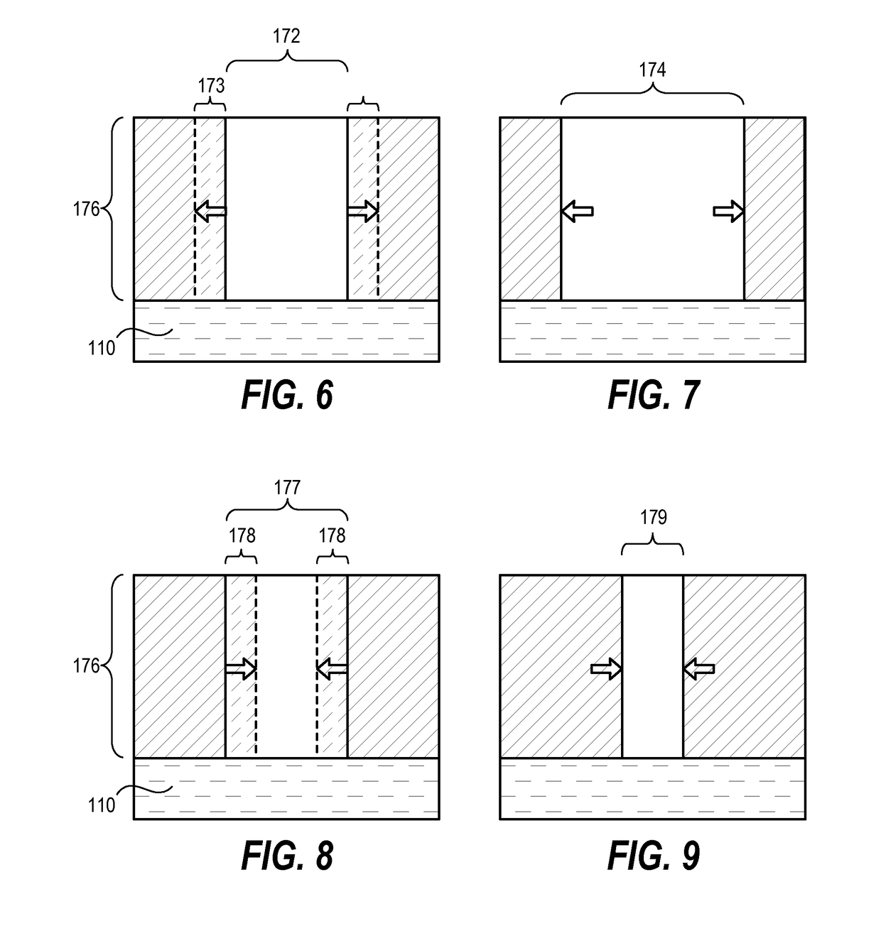
[0020]Techniques herein include systems and methods that provide a spatially-controlled projection of electromagnetic radiation, such as light, onto a substrate as a mechanism of controlling or modulating critical dimensions of various features and structures being micro-fabricated on a substrate. Combining such spatial light projection with photolithographic exposure can achieve significant improvements in critical dimension uniformity across a surface of a substrate. In general, methods herein include patterning processes that identify or receive a critical dimension signature that spatially characterizes critical dimension values that correspond to the substrate. A pattern of electromagnetic radiation is projected onto a patterning film coated on substrate using a digital pixel-based projection system. A conventional photolithographic exposure process is executed subsequent to, or prior to, the pixel-based projection. The patterning film can then be developed to yield a relief pa...


PUM

PropertyMeasurementUnit
wavelengthaaaaaaaaaa

Abstract

Techniques herein include systems and methods that provide a spatially-controlled projection of electromagnetic radiation, such as light, onto a substrate as a mechanism of controlling or modulating critical dimensions of various features and structures being micro-fabricated on a substrate. Combining such spatial light projection with photolithographic exposure can achieve significant improvements in critical dimension uniformity across a surface of a substrate. In general, methods herein include patterning processes that identify or receive a critical dimension signature that spatially characterizes critical dimension values that correspond to the substrate. A pattern of electromagnetic radiation is projected onto a patterning film coated on substrate using a digital pixel-based projection system. A conventional photolithographic exposure process is executed subsequent to, or prior to, the pixel-based projection. The patterning film can then be developed to yield a relief pattern having critical dimensions shaped by both exposure processes.

Description

CROSS REFERENCE TO RELATED APPLICATIONS[0001]The present application claims the benefit of U.S. Provisional Patent Application No. 61 / 932,005, filed on Jan. 27, 2014, entitled “System and Method for Shifting Critical Dimensions of Patterned Films,” which is incorporated herein by reference in its entirety.BACKGROUND OF THE INVENTION[0002]This disclosure relates generally to patterning of substrates including semiconductor substrates such as silicon substrates. This disclosure also relates to processes involved with photolithography including coating and developing films on substrates as part of semiconductor device fabrication. This disclosure particularly relates to controlling dimensions and accuracy of patterned features as part of photolithography and patterning processes.[0003]Photolithography involves coating substrates with films that are sensitive to electromagnetic (EM) radiation, exposing these films to a pattern of a EM radiation to define a latent pattern within the film...

Claims


Application Information

Patent Timeline
Patent Type & Authority Patents(United States)
IPC IPC(8): G03F7/20
CPCG03F7/70425G03F7/70616
Inventor DEVILLIERS, ANTON J.FULFORD, DANIEL
Owner TOKYO ELECTRON LTD
Why Eureka
Try Eureka