Method for monitoring critical sizes of mask plates

A key dimension, mask technology, applied in the photoengraving process of the pattern surface, the original for opto-mechanical processing, optics, etc., which can solve the problem of limited placement, affecting product yield, affecting wafer CD uniformity, etc. problems, to achieve the effect of improving uniformity and improving product yield

Inactive Publication Date: 2018-01-30
SHANGHAI HUALI MICROELECTRONICS CORP
View PDF1 Cites 2 Cited by
  • Summary
  • Abstract
  • Description
  • Claims
  • Application Information

AI Technical Summary

Problems solved by technology

[0004] The traditional detection of CD uniformity is by designing additional specific detection patterns on the mask plate, and then measuring the specific detection patterns, but due to space constraints, the number of these specific detection patterns is very limited, and sometimes it cannot monitor the CD well. Uniformity, especially the uniformity of local CD
If there is a problem with the uniformity of the CD of the mask, it will largely affect the uniformity of the CD on the wafer, which in turn will affect the product yield

Method used


Image

  • Method for monitoring critical sizes of mask plates
  • Method for monitoring critical sizes of mask plates

Examples


Embodiment Construction

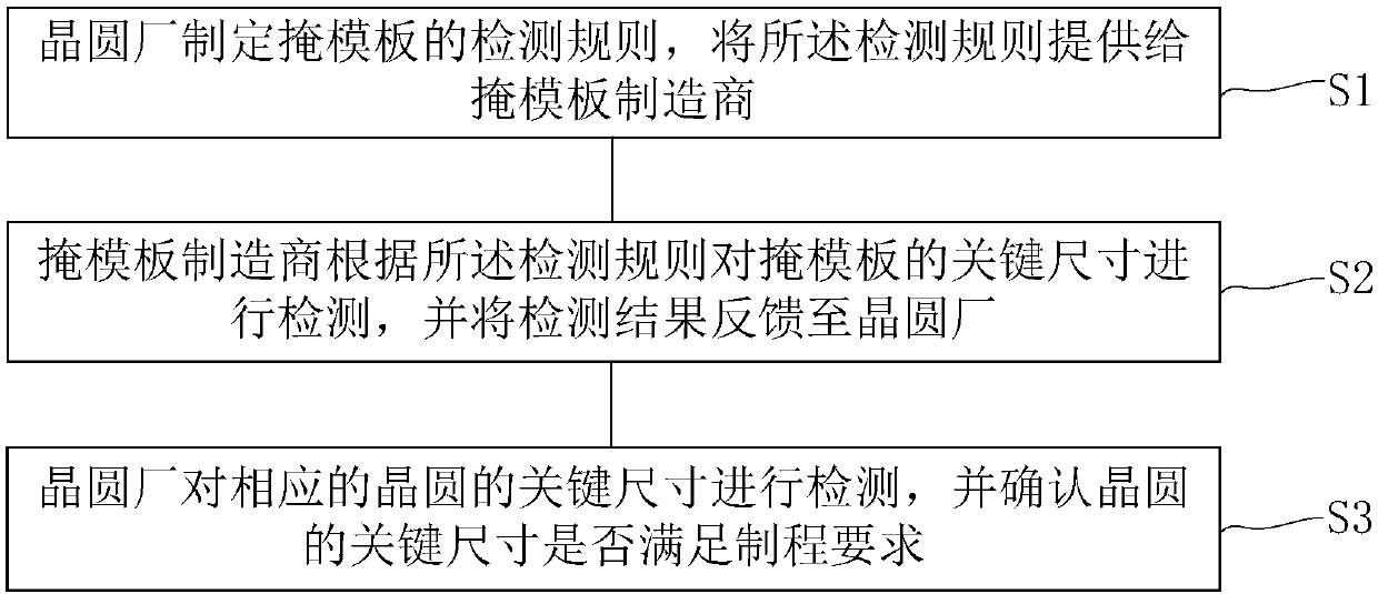
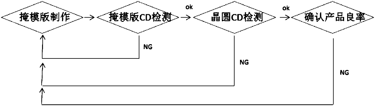
[0020] The method for monitoring critical dimensions of a mask plate of the present invention will be described in more detail below in conjunction with schematic diagrams, wherein a preferred embodiment of the present invention is shown, and it should be understood that those skilled in the art can modify the present invention described here and still implement the present invention beneficial effect. Therefore, the following description should be understood as the broad knowledge of those skilled in the art, but not as a limitation of the present invention.

[0021] In the following paragraphs the invention is described more specifically by way of example with reference to the accompanying drawings. Advantages and features of the present invention will be apparent from the following description and claims. It should be noted that all the drawings are in a very simplified form and use imprecise scales, and are only used to facilitate and clearly assist the purpose of illustr...


PUM


Abstract

The invention provides a method for monitoring critical sizes of mask plates. The method includes formulating detection rules for the mask plates by the aid of wafer factories and providing the detection rules to mask plate manufacturers; detecting the critical sizes of the mask plates by the aid of the mask plate manufacturers according to the detection rules and feeding detection results to thewafer factories; detecting critical sizes of corresponding wafers by the aid of the wafer factories and confirming whether the critical sizes of the wafers meet requirements of manufacture proceduresor not. The method has the advantages that the uniformity of the global and local critical sizes of the mask plates can be effectively monitored and improved by the aid of the method, so that the uniformity of critical sizes of wafer products can be ultimately improved, and the yield of the products can be improved.

Description

technical field [0001] The invention relates to the technical field of integrated circuit design, in particular to a method for integrating hot spots in photolithography process. Background technique [0002] In the semiconductor manufacturing process, integrated circuits with various functions are formed on the semiconductor wafer through a series of processes such as photolithography, etching, doping, film deposition, planarization, and cleaning. The lithography of the heterogeneous area plays a very important role. Due to the needs of the design and manufacturing process, the photolithography process is divided into many process levels, correspondingly requiring many photolithography masks to complete different pattern transfers. [0003] The photolithography mask, also known as photolithography mask or photomask, is a glass substrate that is selectively transparent to exposure light. The quality of the mask greatly affects the transfer of the pattern of the mask to the ...

Claims


Application Information

Patent Timeline
Patent Type & Authority Applications(China)
IPC IPC(8): G03F7/20G03F1/00
Inventor 叶序明毛智彪杨正凯王丹
Owner SHANGHAI HUALI MICROELECTRONICS CORP
Why Eureka
Try Eureka