Mask ROM, method for fabricating the same, and method for coding the same

a mask and mask technology, applied in the field of mask rom, can solve the problems of difficulty in obtaining a proper depth and a proper line width, and achieve the effect of maximizing the integration and packing density of the devi

Inactive Publication Date: 2006-08-31
DONGBU ELECTRONICS CO LTD
View PDF1 Cites 0 Cited by
  • Summary
  • Abstract
  • Description
  • Claims
  • Application Information

AI Technical Summary

Benefits of technology

[0022] An advantage of the present invention is to provide a mask ROM, a method for fabricating the same and a method for coding the same, in which a method for forming the mask ROM maximizes integration and packing density of a device.
[0023] Additional features and advantages of the invention will be set forth in the description which follows, and will become apparent from the description, or may be learned by practice of the invention. The objectives and other advantages of the invention will be realized and attained by the structure and method particularly pointed out in the written description and claims hereof as well as the appended drawings.
[0024] To achieve these and other advantages and in accordance with the purpose of the invention, as embodied and broadly described, a mask ROM includes a semiconductor substrate having a device isolation region and an active region, BN junction regions formed in predetermined portions of the active region, an insulating film formed on a surface of the substrate, first electrode layers formed on predetermined portions of the insulating film, spacers formed at sides of the first electrode layers, and second electrode layers filled between the spacers.
[0025] In another aspect of the present invention, a method for fabricating a mask ROM includes depositing an insulating film on a semiconductor substrate having a device isolation region and an active region, forming BN junction regions by implanting impurity ions into predetermined portions of the substrate, forming first electrode layers by depositing polysilicon on the insulating film and selectively removing the polysilicon, forming spacers at sides of the first electrode layers, and forming second electrode layers between the spacers.
[0026] In another aspect of the present invention, a method for coding a mask ROM includes depositing a base insulating film on the mask ROM, forming base insulating film patterns by selectively removing the base insulating film, and performing a code photolithographic process and an impurity ion implantation process onto portions of the mask ROM exposed by the base insulating film patterns.
[0027] It is to be understood that both the foregoing general description and the following detailed description are exemplary and explanatory and are intended to provide further explanation of the invention as claimed.

Problems solved by technology

However, with the trend towards decreased cell sizes, it is difficult to obtain a proper depth and a proper line width due to a required channel margin.

Method used


Image

  • Mask ROM, method for fabricating the same, and method for coding the same
  • Mask ROM, method for fabricating the same, and method for coding the same
  • Mask ROM, method for fabricating the same, and method for coding the same

Examples


Embodiment Construction

[0036] Reference will now be made in detail to exemplary embodiments of the present invention, examples of which are illustrated in the accompanying drawings. Wherever possible, the same reference numbers will be used throughout the drawings to refer to the same or similar parts.

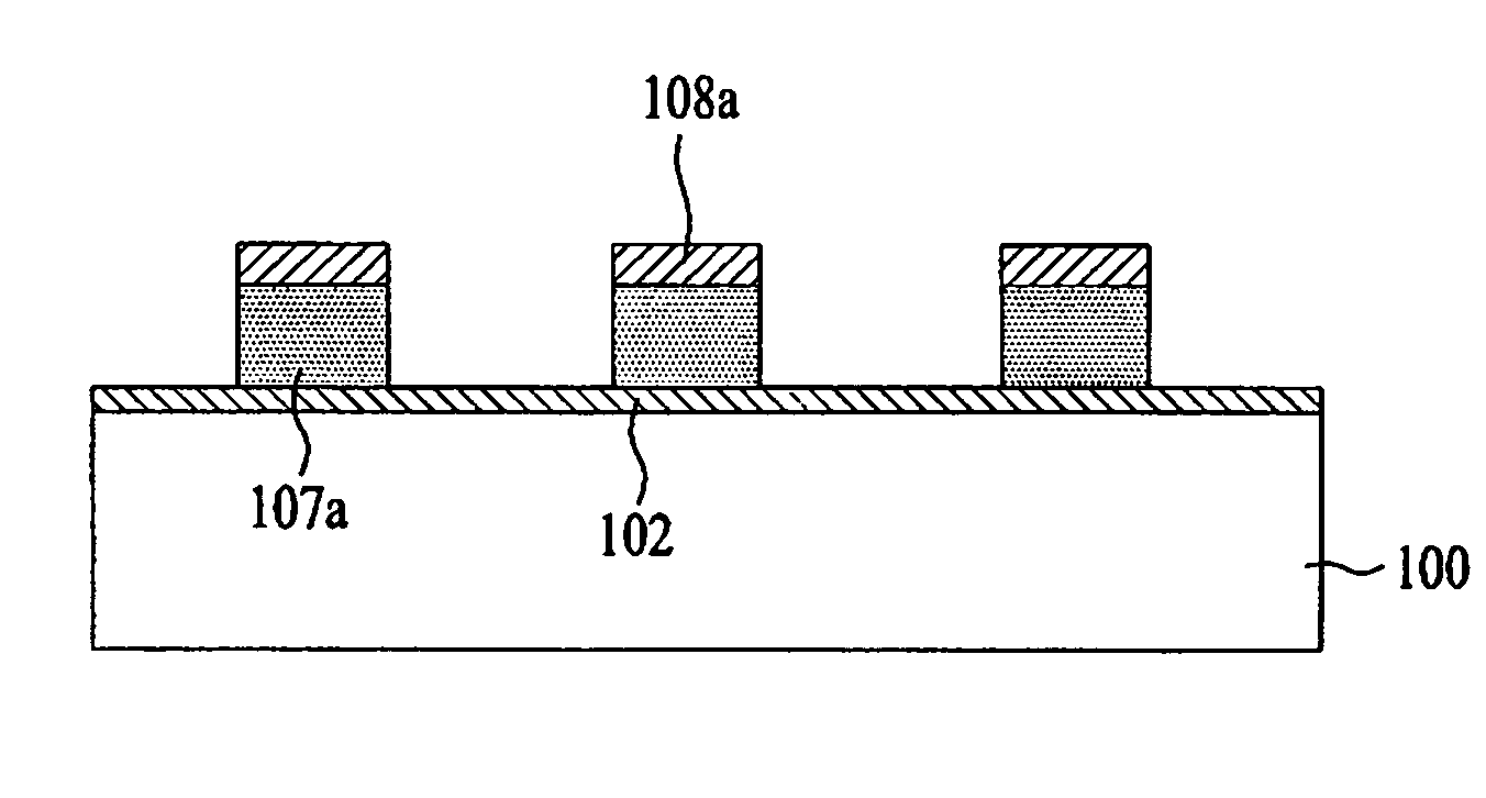
[0037]FIG. 2A is a sectional view illustrating a mask ROM according to an exemplary embodiment of the present invention, viewed from a Bit-Line direction, and FIG. 2B is a sectional view illustrating the mask ROM, viewed from a Word-Line direction.

[0038] As shown in FIGS. 2A and 2B, a mask ROM includes a substrate 100 defined by an isolation oxide film (not shown) and an active region, BN junction regions 106 formed in predetermined portions of the active region, a buffer oxide film 102 formed on an entire surface of the substrate 100, first electrode layers 107a formed on predetermined portions of the buffer oxide film 102, spacers 109 formed at sides of the first electrode layers 107a, and second electro...


PUM


Abstract

A mask ROM, a method for fabricating the same and a method for coding the same are disclosed. The method for forming the mask ROM maximizes packing density and integration of a device. The mask ROM includes a semiconductor substrate having a device isolation region and an active region, BN junction regions formed in predetermined portions of the active region, an insulating film, first electrode layers formed on predetermined portions of the insulating film, spacers formed at sides of the first electrode layers, and second electrode layers between the spacers.

Description

[0001] This application claims the benefit of Korean Patent Application No. 10-2004-0116149, filed on Dec. 30, 2004, which is hereby incorporated by reference for all purposes as if fully set forth herein. BACKGROUND OF THE INVENTION [0002] 1. Field of the Invention [0003] The present invention relates to a semiconductor device, and more particularly, to a mask ROM, a method for fabricating the same and a method for coding the same. The method for forming the mask ROM maximizes integration and packing density of a device. [0004] 2. Discussion of the Related Art [0005] Generally, a flat ROM device is made by a method for fabricating a semiconductor device. That is, the flat ROM device is so-named because its Bit-Line and Word-Line are formed at a step lower than that of other memory devices. A mask ROM is made as a desired cell that is selectively coded with ‘0’ or ‘1’ by a mask process. [0006] A related art mask ROM and a method for fabricating the same will be described. [0007]FIG....

Claims


Application Information

Patent Timeline
Patent Type & Authority Applications(United States)
IPC IPC(8): H01L21/8234H01L29/76
CPCH01L27/112H01L27/11253H10B20/38H10B20/00
Inventor KIM, HEUNG JIN
Owner DONGBU ELECTRONICS CO LTD
Why Eureka
Try Eureka