
Electronic apparatus system with master node and slave node

Inactive Publication Date: 2006-09-07
FUJITSU LTD
View PDF3 Cites 10 Cited by
  • Summary
  • Abstract
  • Description
  • Claims
  • Application Information

AI Technical Summary

Benefits of technology

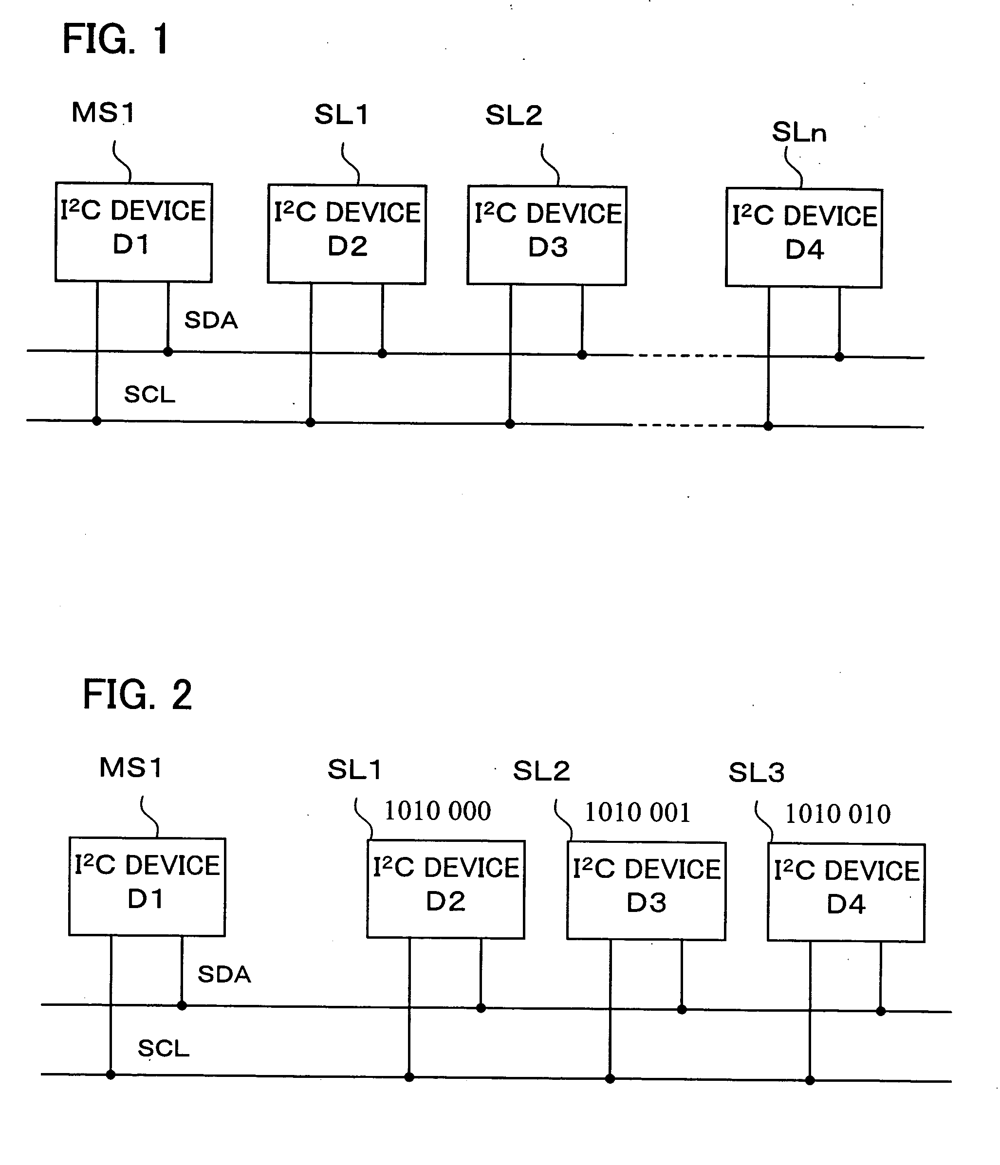
[0015] It is therefore the object of the present invention to provide an electronic apparatus system with master nodes and slave nodes, using I2C slave address allocation for avoiding wrong setting of access destinations due to above wrong address generation.
[0020] The present invention thus allows wrong addressing due to a one-bit error to be avoided, false operation of unintended devices to be avoided, and credibility of a communication system to be improved.

Problems solved by technology

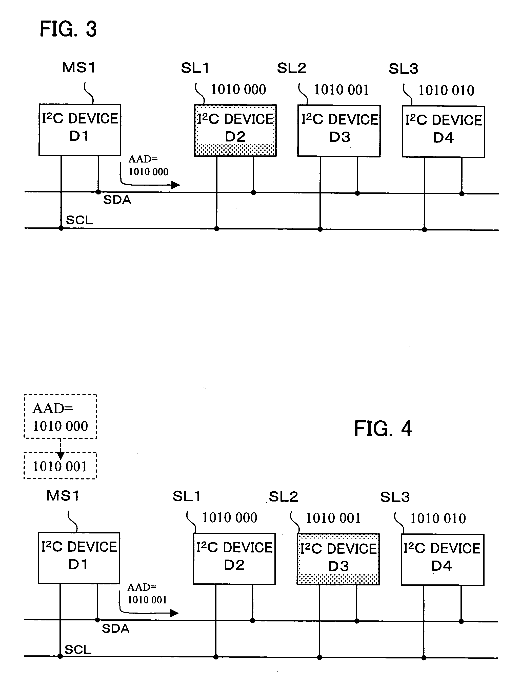
However, due to bugs in firmware, defects in wring or the like, an unintended slave address may be issued by one-bit modification.
If the I2C device SL1 is responsible to control the system, operation of the system is not guaranteed.
For example, if the device has switch functions such as activating power-on or power-off processing, system operation is significantly affected.

Method used


Image

  • Electronic apparatus system with master node and slave node
  • Electronic apparatus system with master node and slave node
  • Electronic apparatus system with master node and slave node

Examples


embodiment 1

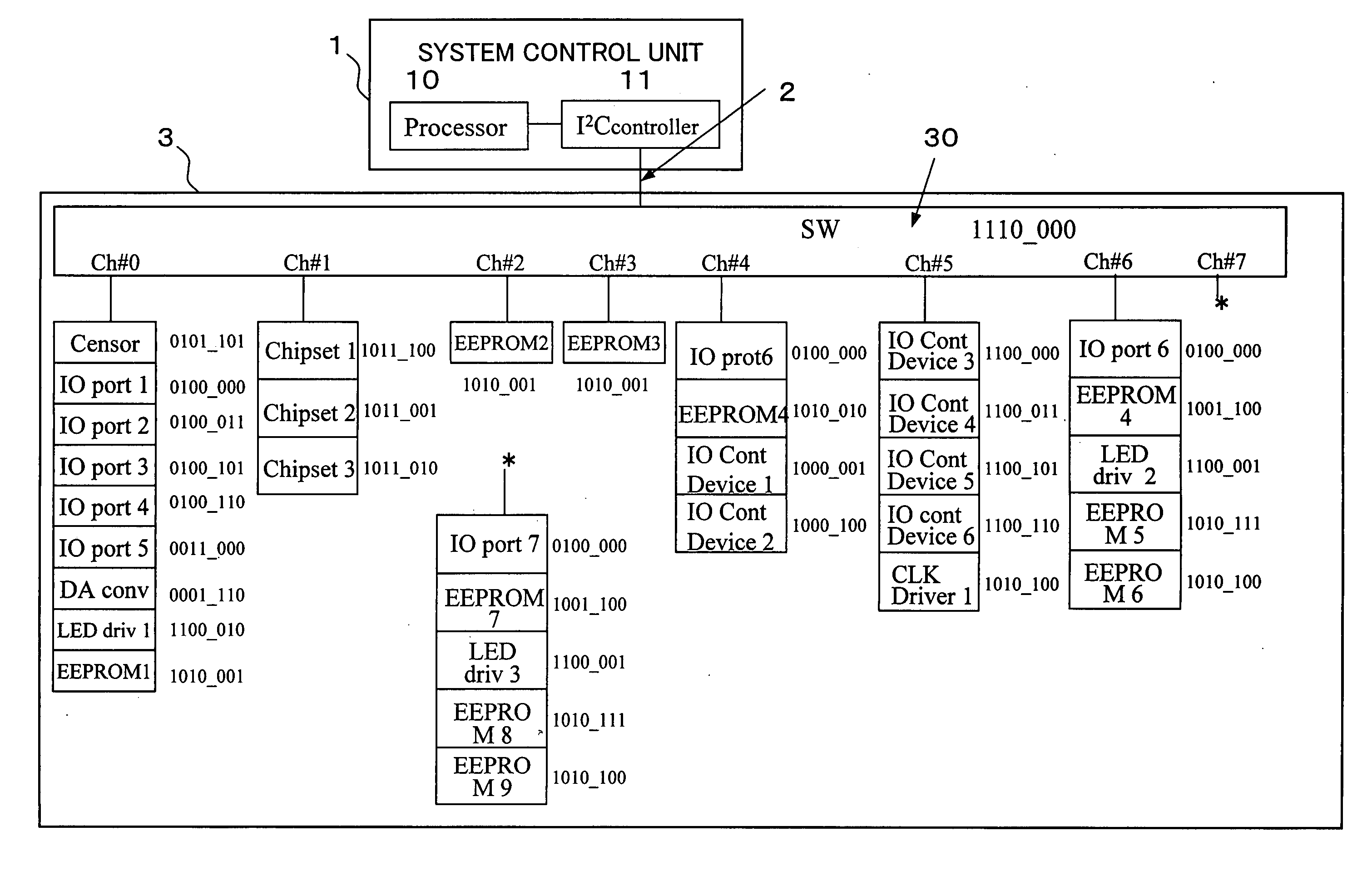
[0035]FIG. 7 is a first embodiment structure block diagram of an information processing system to which the present invention is applied.

[0036] The information processing system shown in FIG. 7 is an example of a server system and has a system control unit 1 controlling the entire system, and an IO board 3 connected to the system control unit 1 through an I2C interface 2 and corresponding to an input-output device unit of the server system.

[0037] The IO board 3 is mounted with various I2C devices for controlling and monitoring, chip sets which can be controlled by I2C, and an IO controller device. On the other hand, the system control unit 1 is mounted with a processor 10 for monitoring and controlling the system, and an I2C controller 11 connected to the processor 10 for controlling the I2C devices.

[0038] The I2C controller 11 is connected to the I2C devices on the IO board 3 through the I2C interface and controls the I2C devices on the IO board 3 by the processor 10 of the syst...


PUM


Abstract

An electronic apparatus system is disclosed that comprises at least one (1) master node; and a plurality of slave nodes connected to the at least one (1) master node via an I2C interface, wherein each of the plurality of slave nodes is set to a slave address with an address distance of two (2) bits or greater with respect to one another.

Description

CROSS-REFERENCE TO RELATED APPLICATIONS [0001] This application is based upon and claims the benefit of priority from the prior Japanese Patent Application No. 2005-62998, filed on Mar. 7, 2005, the entire contents of which are incorporated herein by reference. BACKGROUND OF THE INVENTION [0002] 1. Field of the Invention [0003] The present invention relates generally to a method of setting addresses in an electronic apparatus system with master nodes and slave nodes. More particularly, the present invention relates to address setting of slave nodes in an electronic apparatus system connecting at least one (1) master node with a plurality of slave nodes by use of a bus serial communication system. [0004] 2. Description of the Related Art [0005] As a system connecting many devices or circuit boards with a common bus, a configuration is known which connects at least one (1) master node with a plurality of slave nodes by use of a bus serial communication. For such a configuration, it is...

Claims


Application Information

Patent Timeline
IPC IPC(8): G06F13/00
CPCG06F13/4291G06F13/00G06F13/14
Inventor HATAMORI, SHUEI
Owner FUJITSU LTD
Learn More